Prototype, Design, and Analysis of SIW based Microstrip Tapered Transmission Line
This example shows how to design and analyze a Substrate Integrated Waveguide (SIW) microstrip transmission line using Gerber files.
High performance microwave components can be designed using a novel approach called the Substrate Integrated Waveguide (SIW) technology. This approach combines the advantages of planar technology, such as low fabrication costs, with the low loss inherent to the waveguide solution.
This SIW tapered transmission line model is intended to operate in the microwave frequency range of 10GHz to 15 GHz [1] .
Define Parameters
Below is the schematic diagram of SIW based microstrip tapered transmission line model.
![]()
L   = 40.016e-3;
Wt  = 3.81e-3;
W   = 12e-3;
PW  = 2.46e-3;
L1  = 2.1e-3;
PL  = 6e-3;
gndW = W;
gndL = L+(2*L1)+(2*PL);
% define substrate
h = 0.8e-3;
sub = dielectric('Name',{'duriod'},'EpsilonR',2.2,'LossTangent',0,'Thickness',h);
Create and Analyze SIW Based Tapered Transmission Line
Use the defined parameters to create the microstrip transmission line. A tapered section is used to match the impedance between a 50 Ω microstrip line in which quasi-TEM and TE10 mode are the dominant mode and their electric current distributions are approximate in the profile of the structure are shown.
Create the model using a pcbComponent object and visualize it using the show function.
% Create the tapered planar microstrip line trace
trace1 = traceRectangular('Length',L,'Width',W);
overlapDelta = 1e-7;
v = [-L/2+overlapDelta, Wt/2, 0; -(L/2+L1+overlapDelta), PW/2, 0; -(L/2+L1+overlapDelta),-PW/2,0;-L/2+overlapDelta, -Wt/2, 0];
trace2 = antenna.Polygon('Vertices',v);
trace3 = antenna.Polygon('Vertices',-v);
Port1  = traceRectangular('Length',PL,'Width',PW,'Center',[-gndL/2+PL/2,0]);
Port2  = traceRectangular('Length',PL,'Width',PW,'Center',[gndL/2-PL/2,0]);
Mtrace = trace1+trace2+trace3+Port1+Port2;
In order to build the PCB model, use a pcbComponent object. Mtrace created above will be the top layer on the rectangular SIW.
p = pcbComponent;
p.BoardThickness = h;
gnd = traceRectangular('Length',gndL,'Width',gndW,'Center',[0,0]);
p.BoardShape = gnd;
p.Layers = {Mtrace,sub,gnd};
Define feed and via locations. The FeedLocations and ViaLocations properties are each an array of four elements, in which the 1st and 2nd elements define the x and y co-ordinates, and the 3rd and 4th elements define the layers of connection.
% Define Feed location
p.FeedDiameter = PW/2;
p.FeedLocations = [-gndL/2,0,1,3;gndL/2,0,1,3];
p.ViaDiameter = 1e-3/2;
% Define Via location
offset = 0.5e-3;
viax = -L/2+offset;
viay = -W/2+offset;
for i=1:40
    viaSp = 0.5e-3;
    ViapointX(i) = viax + (i-1)*(viaSp)+(i-1)*(p.ViaDiameter);
    ViapointY(i) = viay;
    layer1(i) = 1;
    layer2(i) = 3;
    Viapoint1     = [ViapointX' ViapointY' layer1' layer2'];
end
for i=1:40
    viaSp = 0.5e-3;
    ViapointX1(i) = viax + (i-1)*(viaSp)+(i-1)*(p.ViaDiameter);
    ViapointY1(i) = -viay;
    layer11(i) = 1;
    layer21(i) = 3;
    Viapoint2     = [ViapointX1' ViapointY1' layer11' layer21'];
end
p.ViaLocations = [Viapoint1;Viapoint2];
figure; show(p);

Use the sparameters function to compute the s-parameters in the frequency range of 10 - 15 GHz and plot it.
freq = linspace(10e9,15e9,31);
spar = sparameters(p,freq);
figure; rfplot(spar,[2 1],1)
axis tight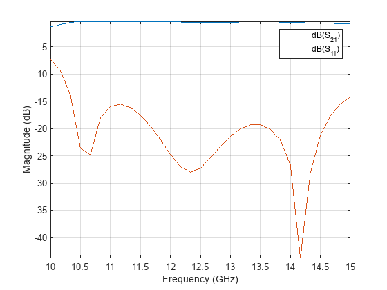
It is observed from the plot that the reflection coefficient S11 is less than -14 dB above 10.3 GHz, and the transmission coefficient S21 is around -0.3 dB to -0.7 dB across the entire band.
Prototype the model using Gerber files
Gerber files are open ASCII vector format files that contain information on each physical board layer of the PCB design. Circuit board objects, like copper traces, vias, pads, solder mask and silkscreen images, are all represented by series of coordinates. These files are used by PCB manufacturers to translate the details of the design into the physical properties of the PCB.
To generate these files, two additional pieces of information are required apart from the PCB design. The first is the type of connector to be used and the second is the PCB manufacturing service/viewer service. The type of RF connector determines the pad layouts on the PCB. The RF PCB Toolbox™ provides a catalog of PCB services and RF connectors. The PCB services catalog supports, configuring the Gerber file generation process for manufacturing as well as for online viewer-only.
Generation of Gerber files
Gerber files contain the collection of files that describe a Printed Circuit Board (PCB) . Each file describes a specific aspect of the PCB design. For example, .gtl and .gbl files contain the information about the metal regions corresponding to the signal and ground that are filled with copper traces. Similarly, .gts and .gbs files hold the information about the solder mask, which is applied to protect and insulate the metal regions. Design information is encoded into the silkscreen layer designated by .gto and .gbo files.
To understand the generation process for these files, use gerberWrite. After generating the Gerber files, you can view them using any third-party online Gerber viewer and render the design.
In this example, the Ucamco Online Gerber Viewer is used to visualize the generated Gerber files.
Online viewer for Gerber files
The PCB model is then passed to a PCBWriter object for Gerber file generation.
PW = PCBWriter(p);
PW.UseDefaultConnector = 0;
Using the PCBWriter created above, run the gerberWrite command to generate the Gerber files for the SIW model. The generated Gerber files are automatically packaged into a ZIP archive and saved in the MATLAB workspace under a folder named "untitled".
gerberWrite(PW)
Once the Gerber files are generated, you can upload—or simply drag and drop—them into the Ucamco Online Gerber Viewer, as shown below. You may also use any other Gerber visualization tool to inspect individual PCB layers and validate the overall design.
![]()
Once the Gerber files are uploaded into the Ucamco Online Gerber Viewer, the individual PCB layers are displayed in the viewer panel as shown below. By default, the viewer assigns standard colors to each layer; however, you can modify these colors using the color‑selector icons next to each file in the layer list.
Adjusting the colors helps improve contrast between layers and enhances the overall visualization of the SIW structure, drill patterns, and metal regions.
![]()
![]()
Reference
Bouchra Rahal*,et.al,"SUBSTRATE INTEGRATED WAVEGUIDE POWER DIVIDER, CIRCULATOR AND COUPLER IN [10-15] GHZ BAND", International Journal of Information Sciences and Techniques,* DOI:10.5121/ijist.2014.4201 , March, 2015.