C28x/C29x CMPSS
R2026bCompare two input voltages on comparator pins
C28x/C29x CMPSS block
To add a block to a model, double-click the canvas and start typing the block name. Then, select the block from the list.
Libraries:
C2000 Microcontroller Blockset /
F280013x
C2000 Microcontroller Blockset /
F280015x
C2000 Microcontroller Blockset /
F28002x
C2000 Microcontroller Blockset /
F28003x
C2000 Microcontroller Blockset /
F28004x
C2000 Microcontroller Blockset /
F2807x
C2000 Microcontroller Blockset /
F2837xD
C2000 Microcontroller Blockset /
F2837xS
C2000 Microcontroller Blockset /
F2838x /
C28x
C2000 Microcontroller Blockset /
F28p65x
C2000 Microcontroller Blockset /
F28p55x
C2000 Microcontroller Blockset /
F29H85x
Description
The Comparator Subsystem consists of two modules, Comparator High (COMPH) and Comparator Low (COMPL). Each module generates a high digital output when the voltage on the first input pin (positive input) is greater than the voltage on the second input pin (negative input). Each module generates a low digital output when the voltage on the first input pin (positive input) is less than the voltage on the second input pin (negative input).
The second input pin can either be the external pin or the DAC module.
Ports
Input
Output
Parameters
Configuration of GPIO as Analog Pins
For TI F280013x and TI F280015x processors, the following table provides the mapping of GPIO pins that can be used as the analog pins for ADC and CMPSS blocks.
| GPIO | ADC | CMPSS | ||
| Module | Channel | Module | Input | |
| GPIO12 | A | 20 | ||
| C | 20 | |||
| GPIO13 | A | 19 | ||
| C | 19 | |||
| GPIO20 | A | 17 | ||
| C | 17 | |||
| GPIO21 | A | 18 | ||
| C | 18 | |||
| GPIO28 | A | 16 | ||
| C | 16 | |||
| GPIO224 | A | 2 | 1 | Positive |
| C | 9 | |||
| GPIO226 | C | 6 | 3 | Positive |
| GPIO227 | A | 9 | 2 | Positive |
| C | 8 | 4 | Positive | |
| GPIO228 | A | 6 | 1 | Positive |
| GPIO230 | A | 10 | 2 | Negative |
| C | 10 | |||
| GPIO242 | A | 3 | 3 | Negative |
| C | 5 | |||
For TI F28P65x processors, the following table provides the mapping of GPIO pins that can be used as the analog pins for ADC and CMPSS blocks.
| GPIO | ADC | CMPSS | |||
| Module | Channel | Module | Input | ||
| GPIO198 | B | 31 | 11 | Positive | |
| C | 7 | ||||
| GPIO199 | B | 24 | 6 | Positive | |
| C | 0 | 6 | Negative | ||
| GPIO200 | B | 25 | 6 | Positive | |
| C | 1 | ||||
| GPIO201 | C | 9 | 11 | Positive | |
| GPIO202 | C | 8 | 10 | Positive | |
| GPIO203 | B | 30 | 10 | Positive | |
| C | 6 | ||||
| GPIO204 | B | 25 | 2 | Positive | |
| C | 9 | 5 | Negative | ||
| GPIO205 | B | 28 | 5 | Positive | |
| C | 4 | 10 | Negative | ||
| GPIO206 | B | 27 | 3 | Positive | |
| C | 3 | 6 | Negative | ||
| GPIO207 | A | 30 | 7 | Positive | |
| B | 6 | 7 | Negative | ||
| GPIO208 | A | 31 | 3 | Negative | |
| B | 7 | 7 | Positive | ||
| GPIO209 | A | 6 | 7 | Positive | |
| GPIO210 | 4 and 9 | Positive | |||
| A | 7 | 7 | Negative | ||
| GPIO211 | A | 8 | 8 | Positive | |
| C | 24 | ||||
| GPIO212 | A | 9 | 5 | Positive | |
| C | 25 | 8 | Negative | ||
| GPIO213 | A | 10 | 8 | Positive | |
| C | 26 | 8 | Negative | ||
| GPIO214 | A | 11 | 8 | Positive | |
| C | 27 | ||||
| GPIO215 | A | 28 | 5 | Positive | |
| B | 4 | 5 | Negative | ||
| GPIO216 | A | 25 | 5 | Positive | |
| B | 5 | ||||
| GPIO217 | B | 8 | 2 | Positive | |
| C | 28 | 10 | Negative | ||
| GPIO218 | B | 9 | 2 | Positive | |
| C | 29 | 9 | Negative | ||
| GPIO219 | B | 10 | 4 | Positive | |
| C | 30 | 4 | Negative | ||
These pins are configured as analog pins if ADC or CMPSS blocks use them. Do not use a GPIO pin as both a digital and an analog pin. For example, GPIO12 cannot be used in a digital input or digital output block and simultaneously as ADCA input channel 20.
F29H85x CMPSS Input Mux Options
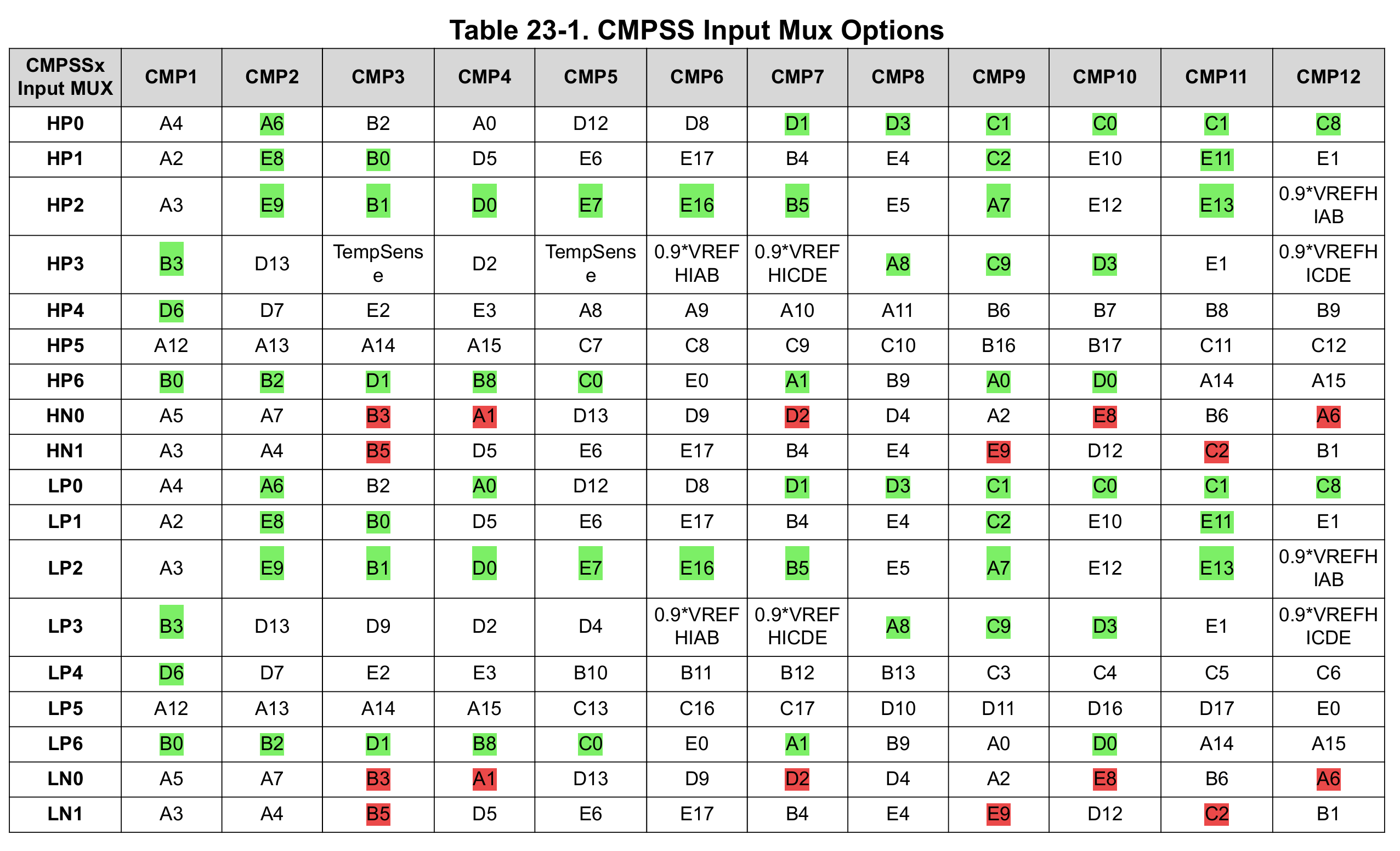
For TI F29H85x processors, the following image shows all available input mux options for CMPSS modules 1–12. The mux index (HP0–HP6, HN0–HN1, LP0–LP6, LN0–LN1) selects which analog pin is connected to the corresponding comparator input. By default, the 0th mux value is selected for all modules. The pins highlighted in green and red are the ones available on the F29H85x HSEC controlCARD.
C28x/C29x Pin MUX Configuration
For processors starting with F28004x, F28P65x, and F29H85x, the positive and negative pin connections for COMPH and COMPL can be configured directly in the Configuration Parameters dialog box under the CMPSS settings. Use the COMPHP pin, COMPHN pin, COMPLP pin, and COMPLN pin drop-downs to select the appropriate analog input pin for each comparator module.
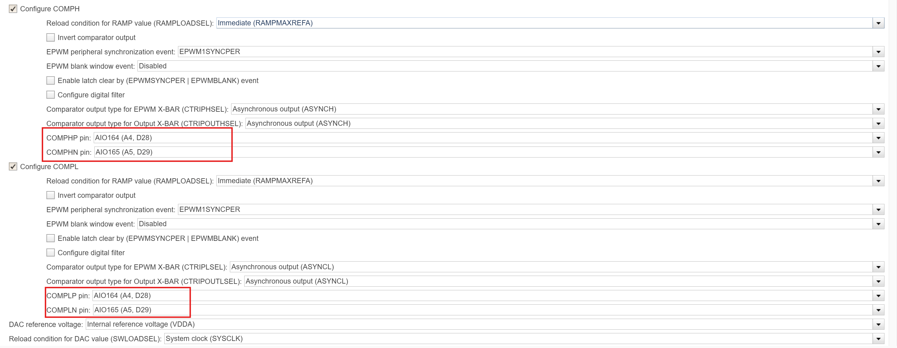
By default, the analog pins are set to the 0th mux value for all CMPSS modules. If the default pin mapping is suitable for your hardware connections, no additional configuration is required. To use a different pin, select the desired pin from the corresponding dropdown in the Configuration Parameters.
Legacy Method
In previous releases, for using pins other than the default ones, the pin mux
selection for CMPSS blocks was done by configuring the
AnalogSubsysRegs registers
(CMPHPMXSEL, CMPHNMXSEL,
CMPLPMXSEL, CMPLNMXSEL;
AGPIOCTRLx in GpioCtrlRegs) using a Register
ReadWrite block in the Initialize Function subsystem or using custom code blocks. This
method is no longer required because the blockset inserts the necessary code when you
choose the option in the Configuration Parameters.
Multi-CPU Usage
On secondary CPUs (such as F28P65x CPU2 and F29H85x CPU2/CPU3), even though the
secondary CPU has access to CMPSS peripheral registers to configure the comparator, the
AnalogSubsysRegs registers that control the analog pin MUX selection
(CMPHPMXSEL, CMPHNMXSEL,
CMPLPMXSEL, CMPLNMXSEL;
AGPIOCTRLx in GpioCtrlRegs) are
not writable from CPU2 or CPU3 — only CPU1 has
write access to these registers. This applies whenever specific analog pins that are AGPIO
or AIO are used. If the pin mux option is selected for a secondary CPU, the CPU2 code uses
IPC to ask CPU1 to configure these registers for the chosen analog pin mux options in the
configuration parameters.

