Prototype IP Core on Zynq with MATLAB FPGA I/O Host Interface
This example shows how to implement a quadrature phase shift keying (QPSK) wireless communication algorithm on a AMD® Zynq® based radio. You deploy QPSK transmitter and receiver algorithms on the hardware and then transmit and receive the stream signals by using the MATLAB® host interface.
QPSK Transmit and Receive on Zynq-Based Radio with MATLAB FPGA I/O Host Interface
Prerequisites
Install and configure these support packages and third-party tools:
HDL Coder™ Support Package for AMD® FPGA and SoC Devices.
Xilinx Vivado®. Use the version in HDL Language Support and Supported Third-Party Tools and Hardware.
MathWorks® firmware image on the SD card of the board. See Guided Hardware Setup for AMD Boards.
Set Up Hardware Board
Download MathWorks® firmware image onto the SD card, then set up the hardware board:
Set the jumper switch positions to [0,0,1,1,0].
Remove the SD card from the host computer and insert it into the Xilinx Zynq ZC706 evaluation kit.
Make the required connections between the hardware board and the development host computer.
Connect the antennas or loopback cable to the add-on card.
Plug the RF add-on card into the LPC FMC connector.
Connect the power cable to the board.
Turn on the power button.
After the board powers on, wait until the LEDs light up. The lights indicate that the radio is ready.
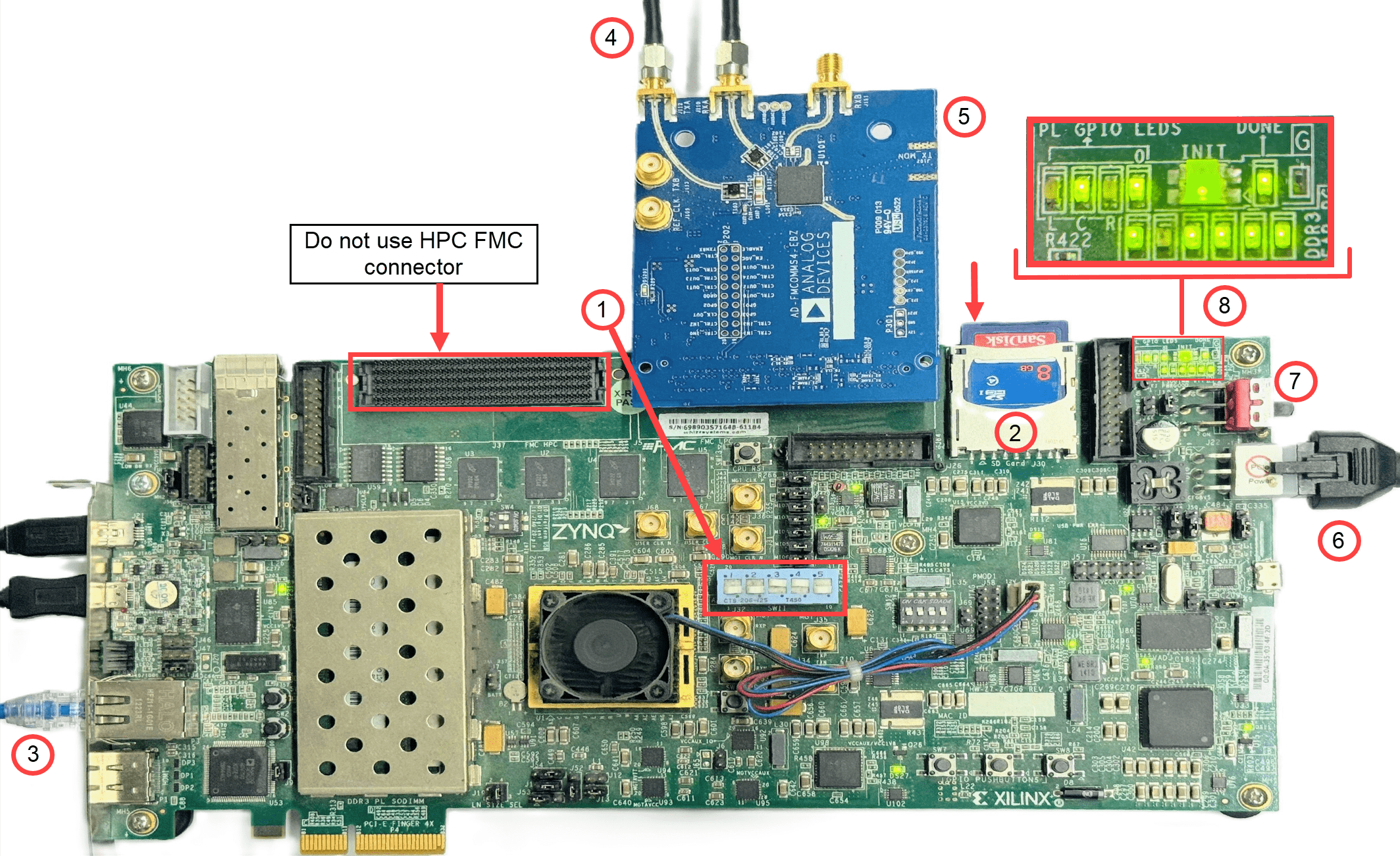
If the LEDs do not light up, verify that:
The jumper switch positions are in the correct position.
The SD card is properly inserted.
If the LEDs do not light up, press the PS-POR button to reset and restart the board.
System Architecture
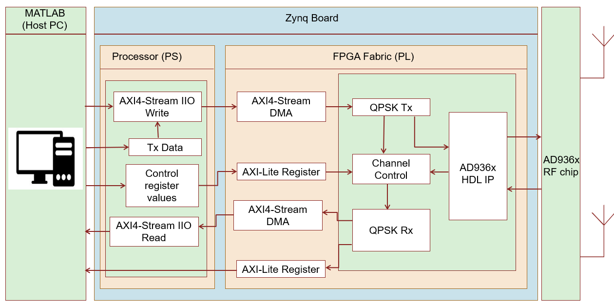
This figure shows the high-level architecture of the QPSK system. The host computer communicates with the FPGA through the processing system on the System on Chip (SoC) board. The host computer can also tune parameters by writing to AXI4-Lite registers in the algorithm IP core.
The hdlcoder_QPSKTxRx_zynqBasedRadio model is a communication system that modulates data using the QPSK technique. The model transmits and receives real-time information.
open_system('hdlcoder_QPSKTxRx_zynqBasedRadio');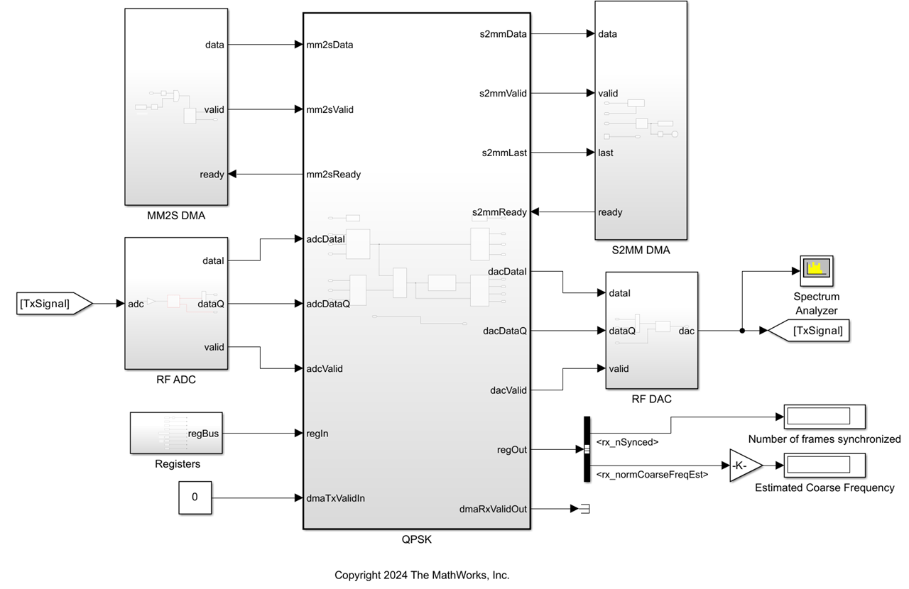
QPSK Transmitter
In the QPSK subsystem, the QPSK transmitter subsystem QPSK Tx gets the input data from the MM2s DMA block. In the QPSK Tx subsystem:
The
Bit Packetizersubsystem collects the data bits, generates the preamble bits, and forms the packet bits. It stores input data and reads it out when required. It also generates thedataReadysignal to indicate if the transmitter is ready to accept input data.The
HDL Data Scramblersubsystem scrambles the data bits of each packet to increase bit transitions and avoid long-running sequences of the same bit.The
QPSK Modulatorsubsystem uses the QPSK Modulator Baseband (Communications Toolbox) block to modulate the preamble and data bits and generate QPSK symbols.The
RRC Transmit Filtersubsystem upsamples and pulse-shapes the QPSK symbols to generate the Tx waveform at a sample rate of four times the symbol rate. The receive filter in the QPSK receiver forms a matched filter to this transmit filter.

QPSK Reciever
In the QPSK subsystem, the QPSK Receiver subsystem QPSK Rx subsystem gets an input signal either from the RF DAC-ADC loopback or directly from QPSK Tx subsystem. In the QPSK Rx subsystem:
The
Digital AGC subsystemcomputes the required gain based on the input signal amplitude. The subsystem then multiplies the resulting gain with the AGC input to generate the AGC output.The
RRC Receive Filtersubsystem uses a Discrete FIR Filter (DSP HDL Toolbox) block with filter coefficients that match filter used for pulse-shaping in the transmitter. TheRRC-matched filtergenerates an RC pulse-shaped waveform, which has zero ISI characteristics at the maximum eye opening in the eye diagram of the waveform. The matched filtering process maximizes the signal-to-noise power ratio (SNR) of the filter output.The
Frequency and Time Synchronizersubsystem performs symbol synchronization, coarse frequency compensation, carrier synchronization, and preamble detection for packet synchronization. It also estimates and resolves the phase ambiguity that the carrier synchronization does not correct.The
QPSK Demodulatorsubsystem uses the QPSK Demodulator Baseband (Communications Toolbox) block to demodulate the packet synchronized symbols and generate bits.The
HDL Data Descramblersubsystem descrambles the demodulated bits to generate the user bits. This subsystem is the same as theHDL Data Scramblersubsystem in theQPSK Txsubsystem.The
Pack Bitssubsystem concatenates the bits to form a packet vector of size 32-by-1 using theScalar to Vector Stream Conversionsubsystem present inside thePack Bitssubsystem

Control Registers
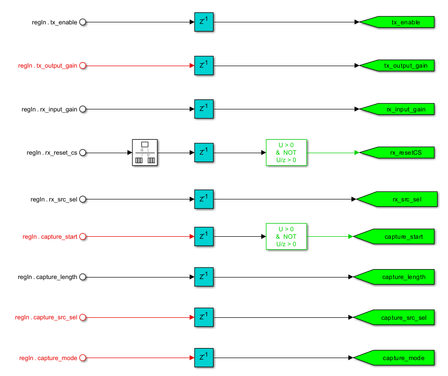
The QPSK subsystem system uses these control registers in the Input Registers subsystem:
Control Register | Description |
|---|---|
| Set this register value to |
| Assign a transmitter gain value to this register that multiplies with data samples before it transmits over the RF AD9361 transmitter chip. |
| Assign a receiver gain value to this register that multiplies with data samples that are received over the RF AD9361 receiver chip. |
| Set the register to |
| Use this register to switch between the different data paths that pass through the QPSK receiver. |
| Set this register value to |
| Use this register to read the length of the frame. |
| Use this register to see the data from different paths for visualization. Set this register to |
| Set this register value to |
Generate the HDL Code and IP Core
1. Set up the Xilinx tool path by using the hdlsetuptoolpath function. For example:
>> hdlsetuptoolpath('ToolName','Xilinx Vivado','ToolPath',vivadopath);
2. Register the custom boards to the MATLAB path:
hdlcoder_amd_examples_root
addpath(fullfile(hdlcoder_amd_examples_root,'ZC706'))
addpath(fullfile(hdlcoder_amd_examples_root,'ipcore'))
3. Open the HDL Workflow Advisor. Right-click on the QPSK subsystem and select HDL Code > HDL Workflow Advisor.
4. In the left pane, click 1. Set Target > 1.2 Set Target Reference Design, and set Target workflow to IP Core Generation and Target platform to Xilinx Zynq ZC706 evaluation kit.
5. In step 1.2, set Reference design to Radio loopback with AXI4-Stream Interface. For this example, you can use the default reference design parameters.
6. In the left pane, click 1.3 Set Target Interface and review the data in the Target platform interface table section. The HDL Workflow Advisor automatically maps the DUT signals to the interface signals in the reference design.
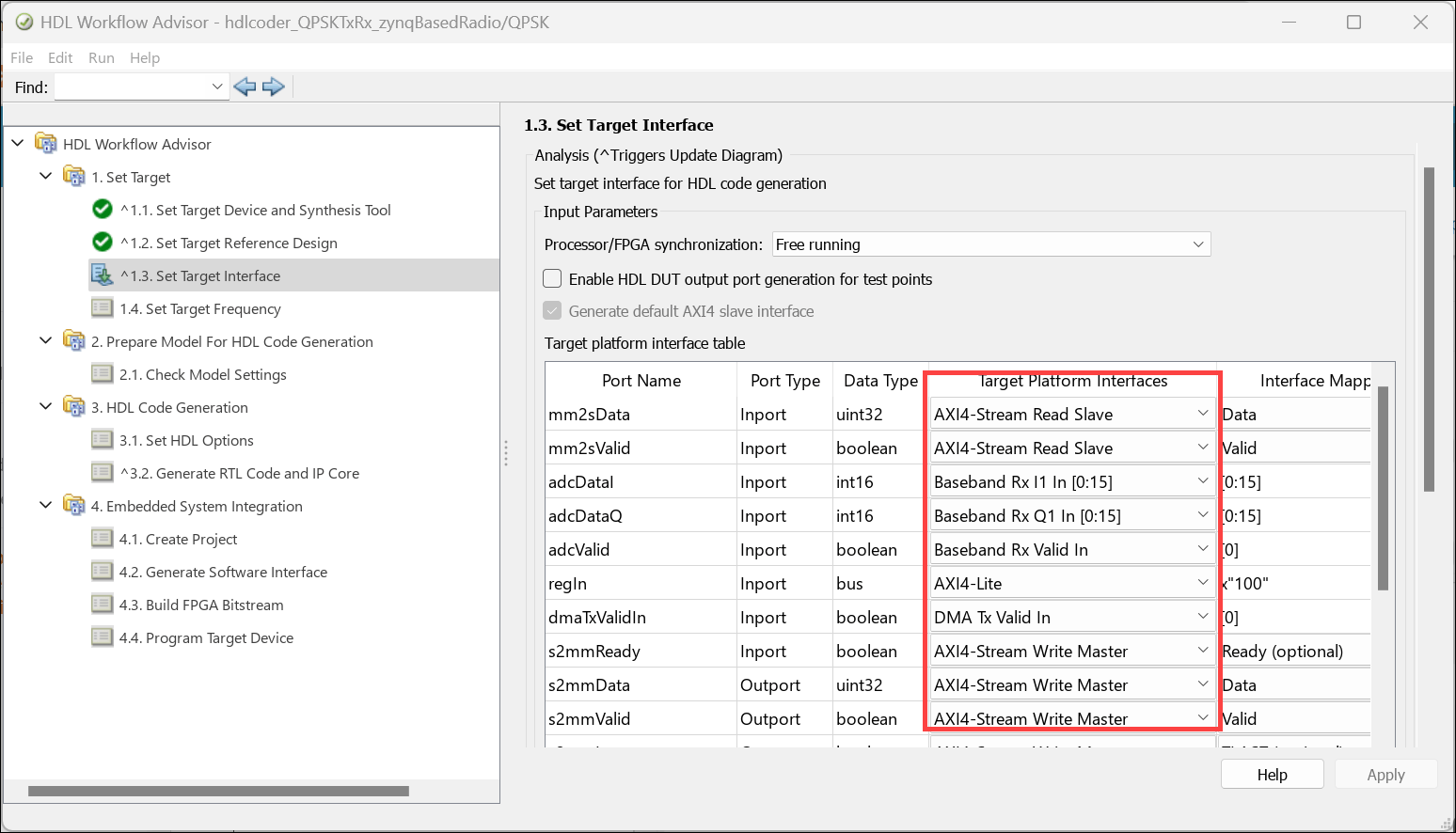
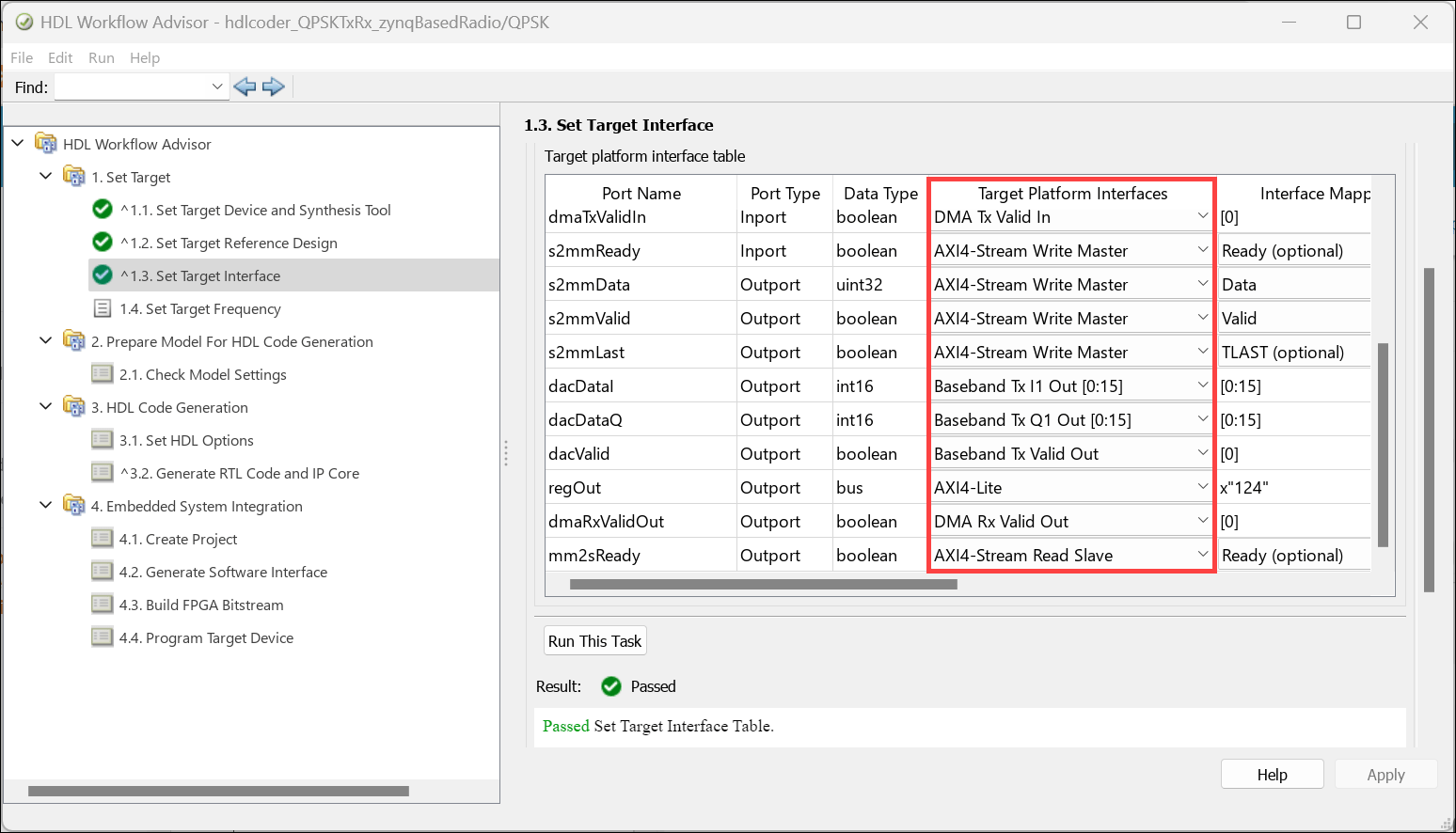
7.In the left pane, click 1.4 Set Target Frequency, and set the Target Frequency (MHz) parameter to the default DUT synthesis frequency.
8. Right-click the 3. HDL Code Generation > 3.2 Generate RTL Code and IP Core task and click Run to Selected Task to generate the HDL code for the IP core.
Code Generation Report
After you generate the custom IP core, the IP core files are in the ipcore folder within your project folder. The HDL code generator generates an HTML custom IP core report with the custom IP core. The report describes the behavior and contents of the generated custom IP core.
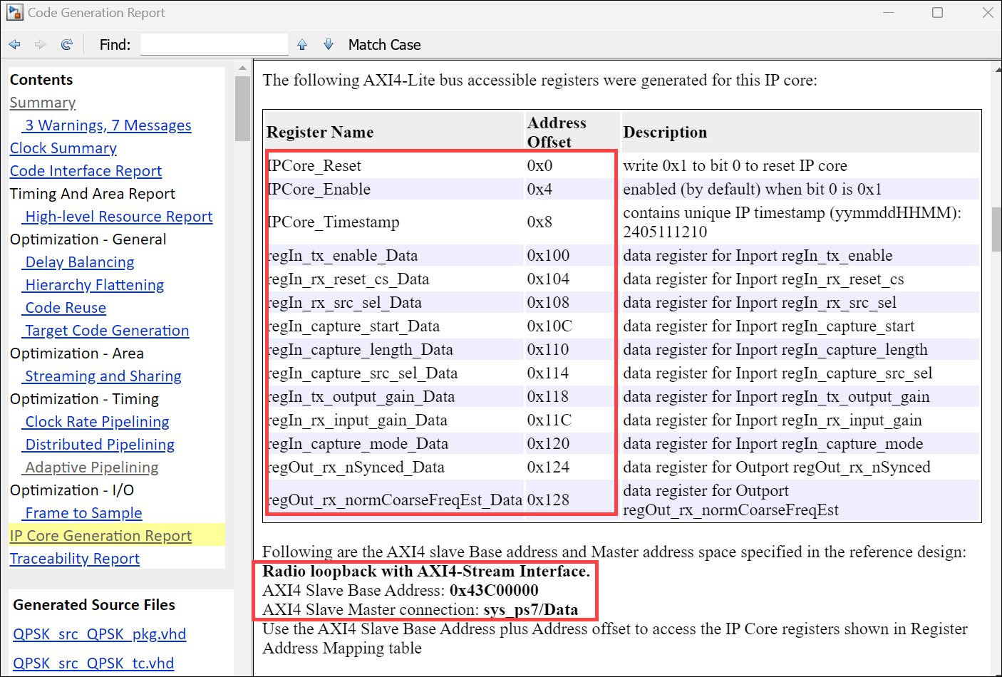
The IP Core Generation Report section contains the details about target platform interface of your model. The figure shows the AXI4 interface mapped to the hdlcoder_QPSKTxRX_zynqBasedRadio model ports. The table in IP Core Generation Report section shows the interface mapping address of each AXI4 slave register. These addresses are used to read the AXI4-slave input registers.
Integrate the IP Core into Embedded System Reference Design
Next, insert your generated IP core into a embedded system reference design, generate an FPGA bitstream, and download the bitstream to the Xilinx Zynq ZC706 hardware.
1. To integrate the HDL Coder IP core into the embedded system, in the HDL Workflow Advisor, click 4. Embedded System Integration > 4.1 Create Project. Click Run This Task. HDL Workflow Advisor creates a Xilinx Vivado project, generates an IP integrator embedded design, and provides links to the Vivado project in the task log.
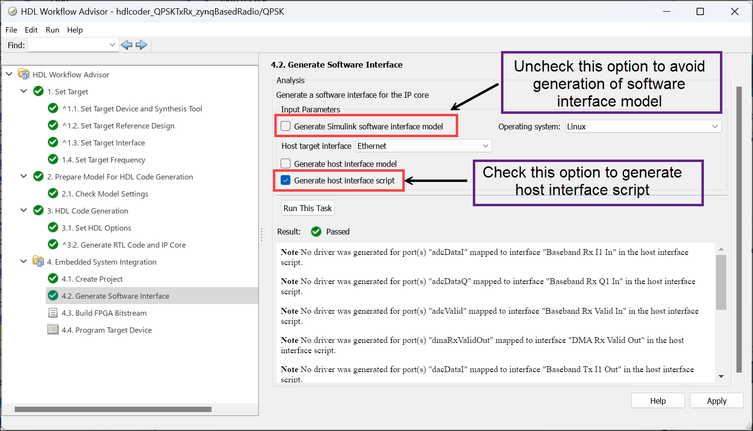
2. In step 4.2 Generate Software Interface, select Generate host interface script. Because the Radio Loopbaack with AXI4 Stream Interface reference design does not support external mode, clear the Generate Simulink software interface model option. Click Run This Task. This step generates two MATLAB files, gs_hdlcoder_QPSKTxRx_zynqBasedRadio_setup and gs_hdlcoder_QPSKTxRx_zynqBasedRadio_interface, in your current folder . You can use these files to prototype your generated IP core directly from MATLAB.
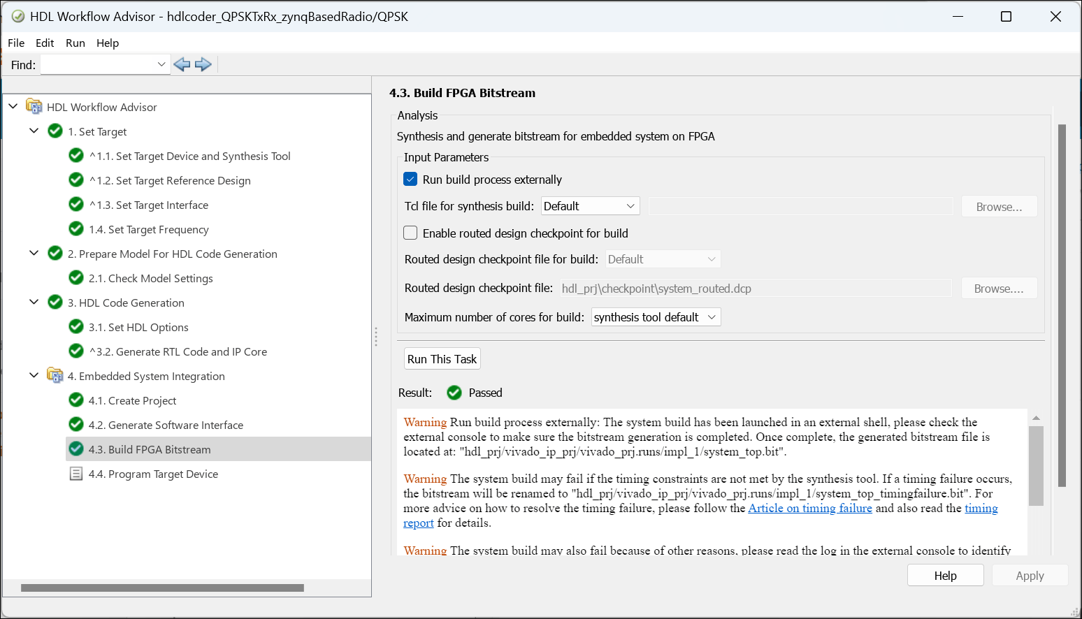
3. Click 4.3. Build FPGA Bitstream. To continue using MATLAB while building the bitstream file, select Run build process externally. Next, click Run This Task. Wait until the external shell displays a successful bitstream build.
Visualize Data Using MATLAB Host Computer
Open the generated host interface script file.
open gs_hdlcoder_QPSKTxRx_zynqBasedRadio_interface.m
Modify the host interface script to:
Create a hardware object to establish a connection to your FPGA.
Deploy the bitstream on hardware.
Configure the SDR hardware object with the required settings.
Write input control signals and stream signals to the PS.
Read the output stream signals from the PS.
By default, the write and read frame length parameters are set to 1024 in gs_hdlcoder_QPSKTxRx_zynqBasedRadio_setup script. This example uses a write and read frame length of 70.
To transmit and receive the streaming data using MATLAB host, modify the host interface script gs_hdlcoder_QPSKTxRx_zynqBasedRadio_interface.m to:
Specify the board credentials such as, IP address, username, and password.
Set the DUT register values by using
writePortcommand.Print transmitted and received data on MATLAB Command Window.
%--------------------------------------------------------------------------
% Host Interface Script
%
% Generated with MATLAB 24.2 (R2024b) at 12:25:10 on 11/05/2024.
% This script was created for the IP Core generated from design 'hdlcoder_QPSKTxRx_zynqBasedRadio'.
%
% Use this script to access DUT ports in the design that were mapped to compatible IP core interfaces.
% You can write to input ports in the design and read from output ports directly from MATLAB.
% To write to input ports, use the "writePort" command and specify the port name and input data. The input data will be cast to the DUT port's data type before writing.
% To read from output ports, use the "readPort" command and specify the port name. The output data will be returned with the same data type as the DUT port.
% Use the "release" command to release MATLAB's control of the hardware resources.
%--------------------------------------------------------------------------

IPAddress = '192.168.1.101'; % Hardware board IP address
Fc = 2.4e9;    % Center Frequency
Fs = 50000000;  % Sampling Frequency
txGain = -10;  % SDR transmitter gain
rxGain = 1;    % SDR receiver gain
FrameSize = 2048;

qpsk_init; % Initialization of model parameters
%% Program FPGA

% Uncomment the lines below to program FPGA hardware with the designated bitstream and configure the processor with the corresponding devicetree.
% MATLAB will connect to the board with an SSH connection to program the FPGA.
% If you need to change login parameters for your board, using the following syntax:

hProcessor = xilinxsoc('192.168.1.101','root','root');
programFPGA(hProcessor, "hdl_prj/vivado_ip_prj/vivado_prj.runs/impl_1/system_top.bit", "devicetree_fmcomms2_axis.dtb");
%% Create fpga object

hFPGA = fpga(hProcessor);
%% Configure SDR SDRTxRx = hdlcoder.sdr('AD936x', ... IPAddress = IPAddress,... CenterFrequency = Fc,... ChannelMapping = [1 2],... BasebandSampleRate = Fs,... TxGain = txGain,... RxGain = rxGain,... SamplesPerFrame = FrameSize); setup(SDRTxRx);
%% Setup fpga object
% This function configures the "fpga" object with the same interfaces as the generated IP core

gs_hdlcoder_QPSKTxRx_zynqBasedRadio_setup(hFPGA);
%% Write/read DUT ports
% Uncomment the following lines to write/read DUT ports in the generated IP Core.
% Update the example data in the write commands with meaningful data to write to the DUT.
%% AXI4-Lite

%Prepare a value for each member of the bus and write it individually.

writePort(hFPGA, "regIn.tx_enable", 1); % One for sending valid data bits to SDR
writePort(hFPGA, "regIn.rx_reset_cs", 0);
writePort(hFPGA, "regIn.rx_src_sel", 1);  % Zero for internal loopback and one for SDR transmission

writePort(hFPGA, "regIn.capture_length", 70); % AXI4 Stream write frame length
writePort(hFPGA, "regIn.capture_src_sel", 0); % Zero for seeing data after QPSK and one for seeing data before QPSK
writePort(hFPGA, "regIn.capture_start", 1); % One to start capturing data from QPSK Rx

writePort(hFPGA, "regIn.tx_output_gain", 1);
writePort(hFPGA, "regIn.rx_input_gain", 1);
writePort(hFPGA, "regIn.capture_mode", 1);
fprintf('\n')
fprintf('####### Transmited Data #######\n')
msgNum = 0;
msg = sprintf('Hello world %d!\n',msgNum);

% Format Tx payload data
txDataBytes = uint8(zeros([1 dataBytesPerPacket]));
txDataBytes(1:length(msg)) = msg;
txDataU32 = typecast(txDataBytes,'uint32');
pause(0.1);
%% AXI4-Stream Read
writePort(hFPGA, "mm2sData", txDataU32);
%% AXI4-Stream Write
[rxData,rxValid] = readPort(hFPGA, "s2mmData");
fprintf('%s\n',char(rxBytes));
if rxValid
    disp('####### Rx Decoded Bytes #########');
    rxBytes = typecast(rxData.','uint8');
    fprintf('%s\n',char(rxBytes));
    idx = 1;
    for ii=1:numel(rxBytes)
        fprintf('%02X ',rxBytes(ii));
        if idx==16
            fprintf('\n');
            idx=1;
        else
            idx=idx+1;
        end
    end
    fprintf('\n');

else
    disp('####### Error: DMA read failed');
end
%% Release hardware resources
release(hFPGA);
delete(hFPGA);
Run gs_hdlcoder_QPSKTxRx_zynqBasedRadio_interface.m.
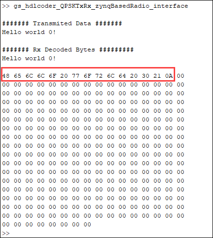
The highlighted part in the output indicates the hexadecimal representation of ASCII codes of the individual characters present in the received data.
In the code generation report, you can see that the AXI4 Slave Base Address is set to 0x43C00000. The data register name for the Inport block regIn_capture_src_selection is regIn_capturesrc_selection and the address offset is 0x114. To read the values stored in this register, and to read the AXI4 lite register values stored in memory, use the devmem command in PuTTY software.
devmem 0x43C00114
![]()
You can see the value set to 0. This can be validated using the value being set to the same register in the host interface script.