Model PLLs in the Phase Domain
R2026bThis example shows how to model a phase-locked loop (PLL) in the phase domain, compare the analytic results to simulation results in the time domain, and identify the advantages and disadvantages of each approach. Most PLL analysis is performed in the phase domain, and this example shows you how to produce a complete analysis using minimum of time and efforts.
The phase domain analysis calculates the PLL transfer function, loop error function, lock time and noise transfer impedances using the Control System Toolbox™. (Automated loop tuning is described in the Tune Phase-Locked Loop Using Loop-Shaping Design example.)
The PLL design and the time domain simulation model were derived from the Phase Noise at PLL Output example.
The general loop filter modeling procedure uses the Mixed-Signal Blockset™ circuit analysis command-line interface (cktconfig and cktssmodel) and was derived from the Circuit Design Details Affect PLL Performance example.
Phase Domain Block Models
This section shows how to create the phase domain models for the individual blocks of an analog phase/frequency locked loop.
The term phase domain refers to the representation of a periodic signal in terms of its phase with respect to an ideal reference with the same period, instead of in terms of its voltage or current as a function of time. Most PLL analyses (in contrast with simulations) treat the PLL as a linear control system in the frequency domain, with the reference signal and the output of the VCO/divider represented in the phase domain.
The Control System Toolbox supports both transfer function (tf) and state space (ss) models. While the tf objects tend to be easier to use, the ss objects are often more accurate at higher frequencies.
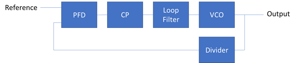
To enable comparison of analysis results to time domain simulation results, this example uses the same design values as the Phase noise at PLL output example.
PllKphi = 5e-3;     % Charge Pump output current
PllKvco = 100e6;    % VCO sensitivity
PllN    = 70;       % Prescaler ratio
PllR2   = 1.33e3;   % Loop filter resistance for second order response (ohms)
PllR3   = 1.7e4;    % Loop filter resistance for third order response (ohms)
PllR4   = 0;        % Loop filter resistance for fourth order response (ohms)
PllC1   = 1.31e-11; % Loop filter direct capacitance (F)
PllC2   = 1.44e-10; % Loop filter capacitance for second order response (F)
PllC3   = 9.41e-13; % Loop filter capacitance for third order response (F)
PllC4   = 0;        % Loop filter capacitance for fourth order response (F)
Reference
The reference signal is assumed to have the same frequency as the ideal reference used to define the phase domain. However, there can be a time-varying phase offset between the reference signal and the ideal reference. This phase offset  , or
, or  in the Laplace domain, is an input to the linear control system.
VCO and Clock Divider
The VCO output phase is the integral of the VCO control voltage.

Or, in the Laplace domain,

From this equation, the statement to construct an ss model of the VCO is
vco = ss(0,2*pi*PllKvco,1,0);
Given a divider ratio PllN (not necessarily integer), the ss object for the divider is
divN = ss(0,0,0,1/PllN);
The VCO also has phase noise at its output, characterized as a phase noise density  , filtered by the closed loop gain of the PLL.
Phase/Frequency Detector (PFD) and Charge Pump (CP)
Given phase domain inputs  and
and  , and maximum output current
  , the average output current of the PFD/CP is:

Or in the Laplace domain:

The CP also has phase noise at its output, characterized as a phase noise density  .
.
Loop Filter
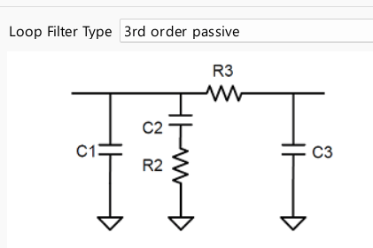
The loop filter presents a transfer impedance  to the CP output, thus converting the CP output current to a control voltage applied to the VCO. [ 1 ] describes a family of widely used second, third and fourth order loop filters. More convenient modeling of this and other loop filter circuit designs using
 cktconfig and cktssmodel is described in the General Loop Filters section below.
The schematic below (from the Mixed-Signal Blockset PLL block mask) shows the 3rd-order passive loop filter topology used in this example. All branches connect to the same charge pump injection node: C1 shunts to ground, C2 in series with R2 provides the stabilizing zero, and R3 in series with C3 provides an extra pole for spur suppression. The VCO control voltage is taken at the R3/C3 junction (node 3).
The second order filter is described by the equation
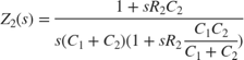
The higher order filters are formed by adding a series R/shunt C section. Given an k-1 order filter design for which Z_(k-1) (s)= (b(s))/(a_(k-1) (s)) , followed by series resistor R_k and shunt capacitor C_k, the transfer impedance of the higher order filter is

One way to transform these equations into an ss object is to calculate the transfer function coefficients and then use the tf2ss function. Given that the filter has nsections sections, with corresponding element values, the procedure is
nsections = 3;
b = zeros(1,nsections+1);
a            = [PllR2*PllC1*PllC2, PllC1+PllC2, 0];
b(end-1:end) = [PllR2*PllC2, 1];
if nsections > 2
    tmp = conv(b, [PllC3 0]);
    a = conv(a, [PllR3*PllC3, 1]) + tmp(end-3:end);
end
if nsections > 3
    tmp = conv(b, [PllC4 0]);
    a = conv(a, [PllR4*PllC4, 1]) + tmp(end-4:end);
end
[A,B,C,D] = tf2ss(b,a);
zlf = ss(A,B,C,D);
The resistors in the loop filter also produce Johnson noise. This noise can be modeled as a noise current that is then applied to a transfer impedance to produce a noise voltage at the output of the loop filter. Given a resistance  , the current spectral density is
  Watts/Hz, where k is Boltzmann's constant and T is the absolute temperature.
The noise transfer impedance calculation follows a very similar process as that for the overall loop filter transfer impedance. However it must be calculated separately for each resistor in the loop filter. The function getNoiseTransferImpedance(R,C,n) included with this example produces an ss model for the device noise transfer impedance of the resistor  .
.
Control Loop Analysis
This section shows how to perform numerous open and closed loop analyses using the phase domain models of the PLL blocks. The process is to first create a closed loop system model and then invoke functions that perform the desired analysis using that model.
Most of the analyses only require a single input, single output model of the PLL, and so you will define that model first. The noise filtering analysis requires a multiple input model, and you will define that in the noise filtering section.
In PLL control loop modeling the divider ratio N is usually kept separate from the gain G due to the PFD/CP, loop filter, and VCO.

The loop transfer function (from reference input to VCO output) is
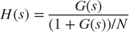
The corresponding MATLAB code is
G = PllKphi/2/pi*zlf*vco;
H = feedback(G,divN);
H.InputName  = 'ref';
H.OutputName = 'out';
Closed Loop Transfer Function
Use the bode function to plot the magnitude and phase of the closed loop transfer function.
NOTE: Configure the bode function to scale the frequency in Hz and not rad/s.
figure(1);
opts = bodeoptions('cstprefs');
opts.FreqUnits = 'Hz';
bodeplot(H,opts);
title('Closed Loop');
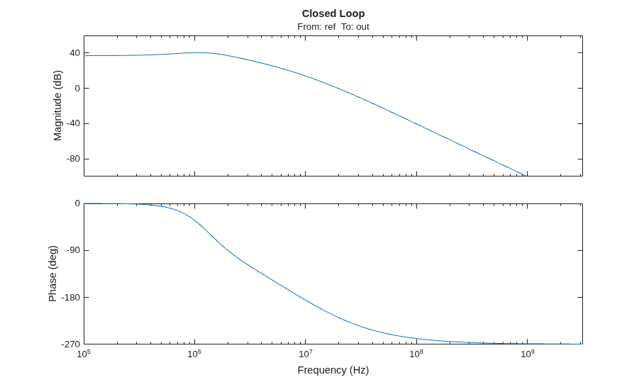
You can also use other variants of the bode function to output results to the workspace for use in other analyses.
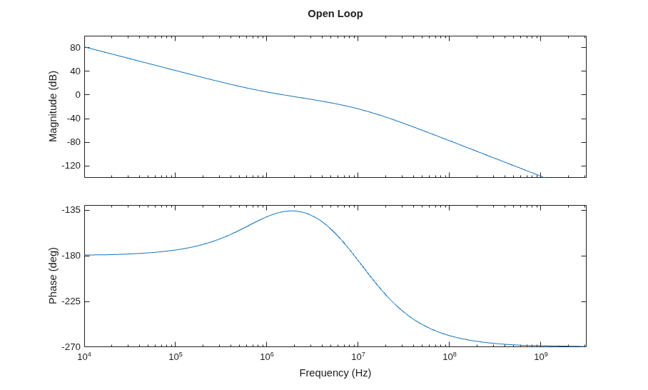
Loop Stability
Use the bode function again to plot the magnitude and phase of the loop gain, only this time use the series function instead of the feedback function
GoverN = series(G,divN);
figure(2);
bodeplot(GoverN,opts);
title('Open Loop');
Lock Time
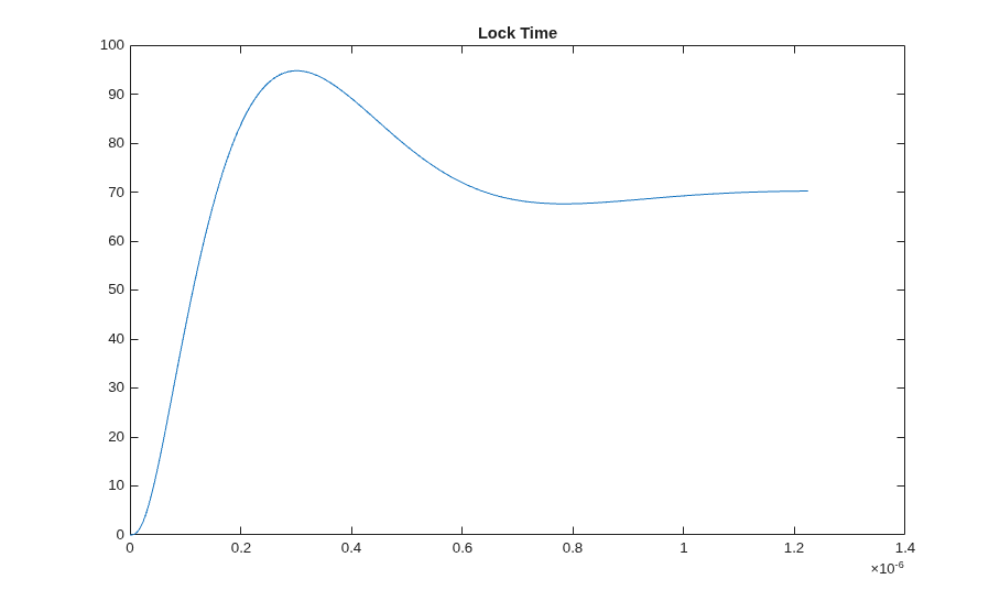
Obtain the loop lock time from the loop step response.
figure(3);
[ystep,tstep] = step(H);
plot(tstep,ystep);
title('Lock Time');
Noise Filtering
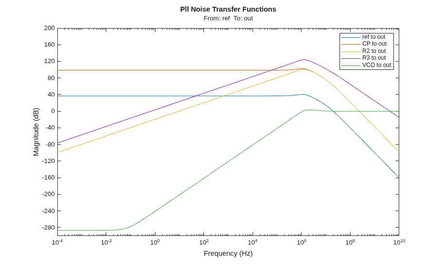
The analysis of noise filtering usually requires multiple inputs- one for each noise source. While such a model could be used for all the analyses presented earlier in this section, that would complicate the coding without providing additional insight. The required block diagram is shown below.
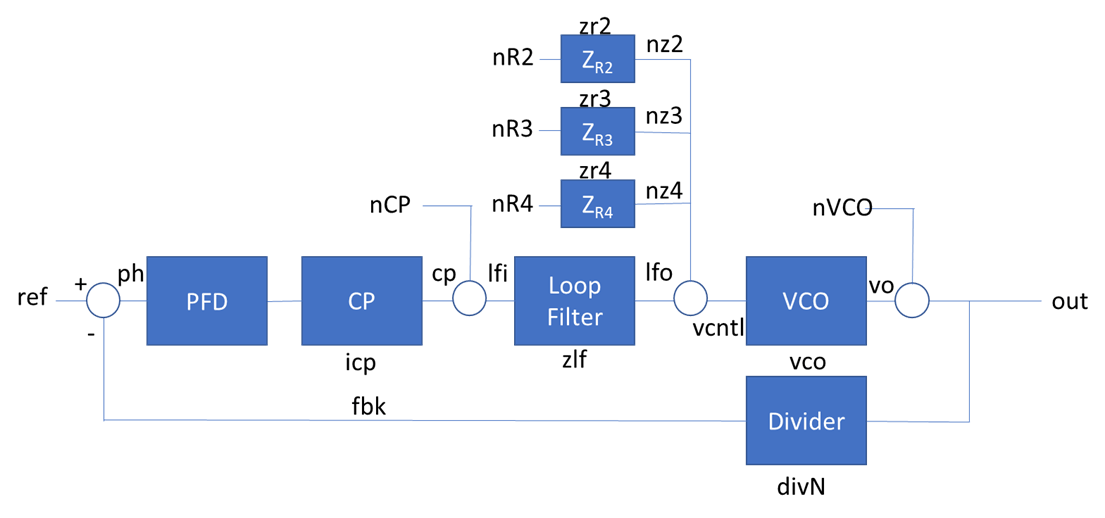
The procedure is to use the connect function to obtain a transfer function from each noise source to the PLL output, apply each of these transfer functions to their respective noise source, and then plot the resulting output noise spectral densities.
The zlf, vco, and divN blocks are already defined.
Define blocks required for noise filtering analysis.
R = [PllR2, PllR3, PllR4];
C = [PllC1, PllC2, PllC3, PllC4];
zr2 = getNoiseTransferImpedance(R,C,2);
zr3 = getNoiseTransferImpedance(R,C,3);
The example loop filter is third order. No need for zr4.
icp = ss(0,0,0, PllKphi/2/pi);
sum1 = sumblk('ph = ref - fbk');
sum2 = sumblk('lfi = cp + nCP');
sum3 = sumblk('vcntl = lfo + nz2 + nz3');
sum4 = sumblk('out = vo + nVCO');
%
zlf.InputName = 'lfi';	zlf.OutputName = 'lfo';
vco.InputName = 'vcntl';	vco.OutputName = 'vo';
divN.InputName = 'out';	divN.OutputName = 'fbk';
icp.InputName = 'ph';	icp.OutputName = 'cp';
zr2.InputName = 'nR2';	zr2.OutputName = 'nz2';
zr3.InputName = 'nR3';	zr3.OutputName = 'nz3';
Connect the PLL as a control system.
Hnoise = connect(icp,zlf,vco,divN,zr2,zr3,sum1,sum2,sum3,sum4,...
                 {'ref','nCP','nR2','nR3','nVCO'},'out');
Href = Hnoise(1,1);
Hncp = Hnoise(1,2);
Hnr2 = Hnoise(1,3);
Hnr3 = Hnoise(1,4);
Hnvco = Hnoise(1,5);
Plot the transfer functions
figure(4);
opts.PhaseVisible = 'off';
bodeplot(Href,Hncp,Hnr2,Hnr3,Hnvco,opts);
title('Pll Noise Transfer Functions');
legend('ref to out','CP to out','R2 to out','R3 to out','VCO to out');
Output Noise Spectral Density
Each of the PLL's internal noise sources can have a flicker noise component (1/f) as well as an additive white Gaussian noise (AWGN) component that is flat with frequency. In this section you will model the combination of these two components as an AWGN process driving a single filter with a gain that is unity at high frequencies but increases as 1/f below a predefined corner frequency. The getFlickerFilter function supplied with this example provides a useful approximation.
The model for the VCO phase noise n_VCO can be obtained from the measured or specified phase noise of the VCO using the process defined for the MSB Ring Oscillator model. This process fits the measured data to a physical model of the VCO (including flicker noise) while avoiding a couple of inaccuracies present in most oscillator phase noise measurements. While the Ring Oscillator model process produces a period offset standard deviation, the application to phase domain modeling requires that the period offset be scaled to a phase offset.
You can derive the n_VCO model for the time domain simulation used in this example using the following steps.
PllFoffset    = [30e3 100e3 1e6 3e6 10e6]; % VCO offset frequencies (Hz)
PllPhaseNoise = [-56 -106 -132 -143 -152]; % VCO output phase noise (dBc/Hz)
CfgRef  = 30e6;          % Reference frequency

f0 = PllN*CfgRef;
[periodjitter,fcorner] = ...
    msblks.VCO.estimatePhaseNoiseCore(f0,PllFoffset,PllPhaseNoise);
phasejitter = 2*pi*f0*periodjitter; % Convert from period jitter to phase jitter
% Scale for the fact that the phase jitter occurs in one VCO output cycle.
n_VCO = ss(0,sqrt(f0)*phasejitter,1,0) * getFlickerFilter(fcorner);
You can model the Johnson current noise in the loop filter resistors by multiplying the broadband current noise density times a flicker filter. Due to the high quality of modern manufacturing, the typical corner frequency for a resistor is somewhere between 1kHz and 10kHz.
kB = 1.3805e-23; % Boltzmann's constant
temp = 273 + 25; % Temperature, in degrees Kelvin for an ambient of 25C
fc_resistors = 3e3; % Typical resistor flicker corner frequency
n_r2 = sqrt(4*kB*temp/PllR2)*getFlickerFilter(fc_resistors);
n_r3 = sqrt(4*kB*temp/PllR3)*getFlickerFilter(fc_resistors);
The CP is an active circuit, and the noise it generates is determined by details of the circuit design and device parameters. Its noise density is best obtained from device data sheets. However at least one version of such data sheet parameters [ 1 ] characterizes the noise at the output of the PLL and not the output of the charge pump.
For the sake of having some sort of model, suppose that
1. In steady state operation, on average one or the other CP output transistor is operating with a duty cycle d. 0.01 < d < 0.1
2. When one of the CP output transistors is on, its  channel conductivity
  is
is  where
where  and the saturation factor
  .
.
3. The channel current integration constant is 
Then the CP current noise spectral density is 
CP_d = 0.03;
CP_A = 4;
CP_VDD = 5;
CP_gamma = 1;
n_CP = sqrt(4*kB*temp*CP_d*CP_gamma*PllKphi/CP_A/CP_VDD)*...
    getFlickerFilter(fc_resistors);
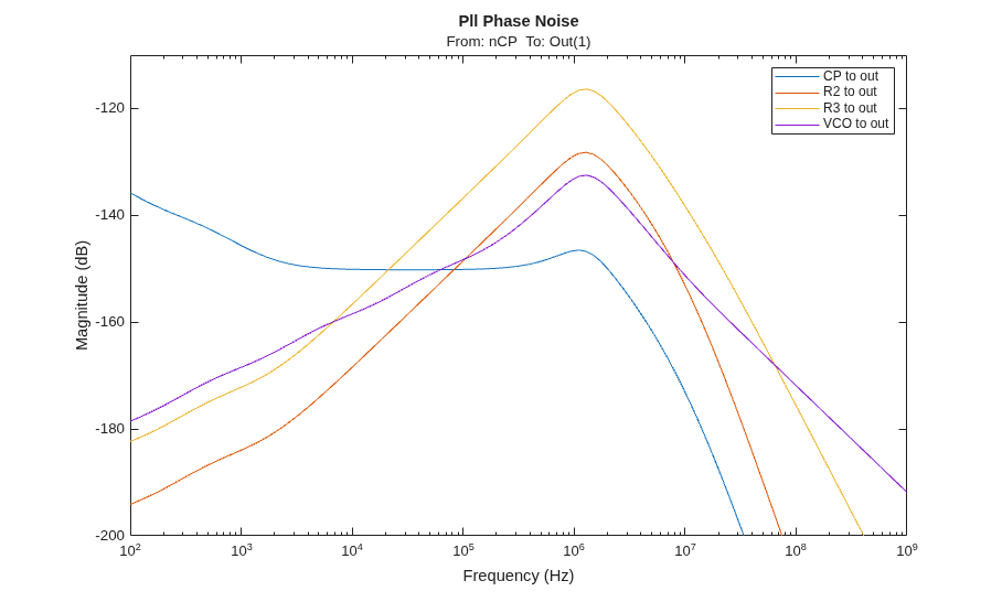
Plot the phase noise contributions for all four noise sources.
figure(5);
opts.PhaseVisible = 'off';
opts.MagLowerLimMode = 'manual';
opts.MagLowerLim = -200;
opts.XLimMode = 'manual';
opts.XLim = [100,1e9];
nout_CP = n_CP*Hncp;
nout_R2 = n_r2*Hnr2;
nout_R3 = n_r3*Hnr3;
nout_VCO = n_VCO*Hnvco;
bodeplot(nout_CP,nout_R2,nout_R3,nout_VCO,opts);
title('Pll Phase Noise');
legend('CP to out','R2 to out','R3 to out','VCO to out');
opts.PhaseVisible = 'on';
opts.MagLowerLimMode = 'auto';
opts.XLimMode = 'auto';
Validate Against estimatePLLPhaseNoise
The entire phase-noise analysis above -- building transfer functions, modeling noise sources with flicker corners, and computing per-source contributions -- can be reproduced in a single call to estimatePLLPhaseNoise. This function builds the same linear phase-domain model internally and returns the noise contributions from all sources. Use it to validate the manual analysis or as a fast design exploration tool.
Internally, estimatePLLPhaseNoise constructs a state-space model of the loop filter using the same parallel topology: the charge pump injects current at the common node where C1, R2+C2, and R3+C3 connect in parallel. This is identical to the transfer impedance  derived above, so both approaches should produce matching results.
vcoPN.f_Hz = PllFoffset;
vcoPN.L_dBc_per_Hz = PllPhaseNoise;

est = estimatePLLPhaseNoise( ...
    Architecture            = "integer-single", ...
    ReferenceFrequency      = CfgRef, ...
    ChargePumpCurrent       = PllKphi, ...
    VCOSensitivity          = PllKvco, ...
    DividerRatio            = PllN, ...
    R2 = PllR2, C1 = PllC1, C2 = PllC2, ...
    R3 = PllR3, C3 = PllC3, ...
    VCOPhaseNoise           = vcoPN, ...
    ChargePumpNoiseDensity  = 4*kB*temp*CP_d*CP_gamma*PllKphi/CP_A/CP_VDD, ...
    ChargePumpFlickerCorner = fc_resistors, ...
    ResistorFlickerCorner   = fc_resistors, ...
    FrequencyOffset         = logspace(5, log10(5e6), 500));
close(gcf);  % Close auto-generated plot; we create a custom overlay below
--- PLL Phase Noise Contribution Summary ---
  [not plotted] Reference - ReferencePhaseNoise not provided
  [not plotted] Divider - DividerPhaseNoise not provided and UseDSMDividerNoise is false
  [not plotted] R4 thermal - R4 is zero (not present)
  [dominant] R3 thermal - 89.9% of total integrated phase noise power
--------------------------------------------
Overlay the manual analysis using the same noise transfer functions computed earlier (Hncp, Hnr3, Hnvco). For the VCO contribution, estimatePLLPhaseNoise uses direct interpolation of the phase noise specification rather than the physical model fit from estimatePhaseNoiseCore. To ensure an apples-to-apples comparison, the manual VCO overlay also uses direct interpolation.
fOffsets = est.FrequencyOffset;
wOffsets = 2*pi*fOffsets;

% CP contribution: noise source through CP-to-output transfer function
[m_cp,~] = bode(nout_CP, wOffsets); m_cp = squeeze(m_cp);
pn_cp_manual = 10*log10(m_cp.^2);

% R3 contribution
[m_r3,~] = bode(nout_R3, wOffsets); m_r3 = squeeze(m_r3);
pn_r3_manual = 10*log10(m_r3.^2);

% VCO: direct interpolation of free-running phase noise specification,
% scaled by x2 to match MSB block internal noise generation convention,
% then filtered by the VCO error transfer function.
vco_freerun = interp1(log10(PllFoffset), PllPhaseNoise, ...
    log10(fOffsets), 'linear', 'extrap');
vco_psd = 2 * 10.^(vco_freerun(:)/10);  % One-sided PSD (MSB convention)
[m_etf,~] = bode(Hnvco, wOffsets); m_etf = squeeze(m_etf);
pn_vco_manual = 10*log10(vco_psd .* m_etf(:).^2);

pn_total_manual = 10*log10(10.^(pn_cp_manual/10) + 10.^(pn_r3_manual/10) + ...
    10.^(pn_vco_manual/10));

figure(8);
semilogx(fOffsets, est.TotalPhaseNoise, 'k', 'LineWidth', 2); hold on;
semilogx(fOffsets, est.VCOPhaseNoise, 'Color', [0.85 0.33 0.1], 'LineWidth', 1.5);
semilogx(fOffsets, est.ChargePumpPhaseNoise, 'Color', [0.93 0.69 0.13], 'LineWidth', 1.5);
semilogx(fOffsets, est.R3PhaseNoise, 'Color', [0.47 0.67 0.19], 'LineWidth', 1.5);
semilogx(fOffsets, pn_total_manual, 'k--', 'LineWidth', 1.5);
semilogx(fOffsets, pn_vco_manual, '--', 'Color', [0.85 0.33 0.1], 'LineWidth', 1);
semilogx(fOffsets, pn_cp_manual, '--', 'Color', [0.93 0.69 0.13], 'LineWidth', 1);
semilogx(fOffsets, pn_r3_manual, '--', 'Color', [0.47 0.67 0.19], 'LineWidth', 1);
hold off;
xlabel('Frequency Offset (Hz)');
ylabel('Phase Noise (dBc/Hz)');
title('Phase Noise: Manual Analysis vs. estimatePLLPhaseNoise');
legend({'est: Total','est: VCO','est: CP','est: R3', ...
    'Manual: Total','Manual: VCO','Manual: CP','Manual: R3'}, ...
    'Location','northeast','NumColumns',2);
xlim([1e5 5e6]);
grid on;
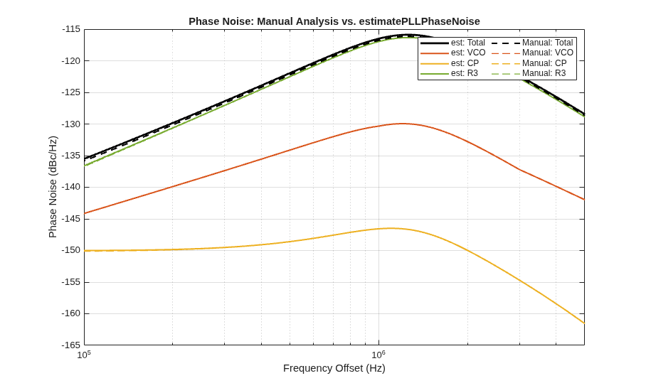
The solid lines (estimatePLLPhaseNoise) and dashed lines (manual analysis) overlap closely, confirming that both approaches produce the same frequency-domain noise budget. Any minor differences arise from the VCO noise model: the manual analysis uses direct interpolation in log-frequency, while estimatePLLPhaseNoise uses an equivalent interpolation internally.
Design Exploration with estimatePLLPhaseNoise
Because estimatePLLPhaseNoise runs in milliseconds, it enables rapid parameter sweeps that would be tedious to set up manually. The following sweep varies the charge pump current - a primary design knob that directly scales the loop gain and bandwidth. Higher widens the loop bandwidth, improving VCO noise suppression at large offsets but increasing the charge pump noise contribution in-band.
Icp_sweep = [1e-3 2.5e-3 5e-3 10e-3];
hFig9 = figure(9);
for i = 1:numel(Icp_sweep)
    Icp_i = Icp_sweep(i);
    est_i = estimatePLLPhaseNoise( ...
        Architecture        = "integer-single", ...
        ReferenceFrequency  = CfgRef, ...
        ChargePumpCurrent   = Icp_i, ...
        VCOSensitivity      = PllKvco, ...
        DividerRatio        = PllN, ...
        R2 = PllR2, C1 = PllC1, C2 = PllC2, ...
        R3 = PllR3, C3 = PllC3, ...
        VCOPhaseNoise       = vcoPN, ...
        ChargePumpNoiseDensity = 4*kB*temp*CP_d*CP_gamma*Icp_i/CP_A/CP_VDD, ...
        ChargePumpFlickerCorner = fc_resistors, ...
        ResistorFlickerCorner = fc_resistors, ...
        FrequencyOffset     = logspace(5, log10(5e6), 300));
    close(gcf);  % Close auto-generated per-call plot
    figure(hFig9);  % Ensure we plot back into Figure 9
    semilogx(est_i.FrequencyOffset, est_i.TotalPhaseNoise, 'LineWidth', 1.5);
    hold on;
end
xlabel('Frequency Offset (Hz)');
ylabel('Phase Noise (dBc/Hz)');
title('Phase Noise vs. Charge Pump Current');
legend(compose("I_{CP} = %g mA", Icp_sweep*1e3), 'Location', 'northeast');
xlim([1e5 5e6]);
grid on;
--- PLL Phase Noise Contribution Summary ---
  [not plotted] Reference - ReferencePhaseNoise not provided
  [not plotted] Divider - DividerPhaseNoise not provided and UseDSMDividerNoise is false
  [not plotted] R4 thermal - R4 is zero (not present)
  [dominant] R3 thermal - 86.5% of total integrated phase noise power
--------------------------------------------


--- PLL Phase Noise Contribution Summary ---
  [not plotted] Reference - ReferencePhaseNoise not provided
  [not plotted] Divider - DividerPhaseNoise not provided and UseDSMDividerNoise is false
  [not plotted] R4 thermal - R4 is zero (not present)
  [dominant] R3 thermal - 88.9% of total integrated phase noise power
--------------------------------------------


--- PLL Phase Noise Contribution Summary ---
  [not plotted] Reference - ReferencePhaseNoise not provided
  [not plotted] Divider - DividerPhaseNoise not provided and UseDSMDividerNoise is false
  [not plotted] R4 thermal - R4 is zero (not present)
  [dominant] R3 thermal - 89.9% of total integrated phase noise power
--------------------------------------------


--- PLL Phase Noise Contribution Summary ---
  [not plotted] Reference - ReferencePhaseNoise not provided
  [not plotted] Divider - DividerPhaseNoise not provided and UseDSMDividerNoise is false
  [not plotted] R4 thermal - R4 is zero (not present)
  [dominant] R3 thermal - 90.4% of total integrated phase noise power
--------------------------------------------
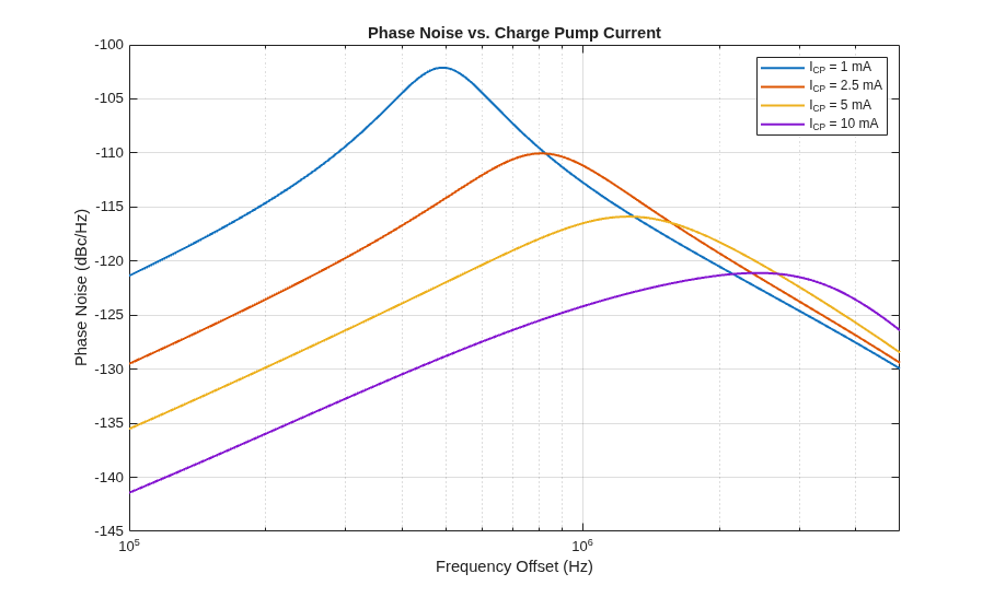
The sweep illustrates a key PLL design trade-off. Increasing widens the loop bandwidth, which suppresses VCO phase noise at higher offsets. However, higher also raises the charge pump noise floor (since CP current noise scales with ), increasing in-band noise. The optimal charge pump current balances these competing effects for a given phase noise specification.
Use the manual phase-domain approach (shown earlier in this example) when you need custom topologies or deep understanding of the control loop. Use estimatePLLPhaseNoise for standard Mixed-Signal Blockset PLL architectures and fast design iteration.
Compare to time domain results
This section compares the phase domain analysis results to the results of a time domain simulation using the model presented in the Phase Noise at PLL Output example. The clearest and most direct approach is to compare the step response predicted by the analysis with the phase lock response produced by the simulation.
The PllPhaseNoiseExample.slx model included with this example is statically configured for the purposes of this section. The workspace output and a CP output monitor port give you access to additional data when performing follow-on investigations such as are suggested in this section and the Compare Z domain with Laplace domain subsection.
Run the time domain simulation and compare the loop lock response to a manually adjusted copy of the phase domain step response.
open_system('PllLoopDynamicsExample.slx');
out = sim('PllLoopDynamicsExample.slx');
figure(6);
plot(out.vco_in.Time,squeeze(out.vco_in.Data));
hold on;
plot(tstep+1.46e-7,0.913/24.7*(ystep-70));
title('Comparison between Simulation and Analysis')
legend('Time domain simulation','Phase domain analysis')
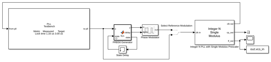
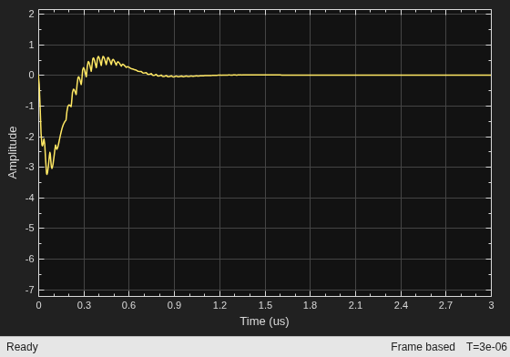
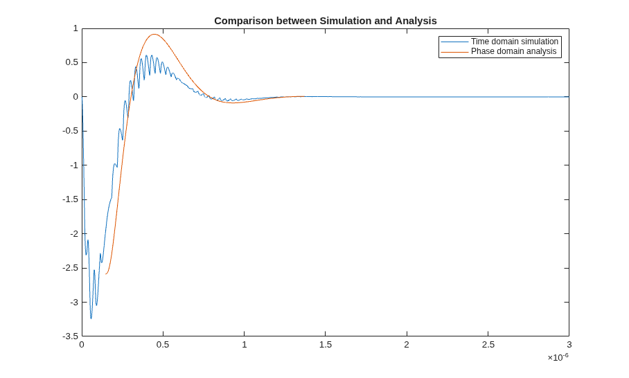
The time domain loop lock response agrees quite well with the phase domain analysis result. It is interesting that there is a portion of the time domain response that precedes the phase domain step response. Using features explained in the following paragraph, you can demonstrate that this phenomenon occurs even for very small phase steps, and is therefore a linear response phenomenon.
As an aid to further study, the reference phase modulator in the model has been configured to produce a PRBS6 modulation with a long enough period to capture the entire step response, and a low enough amplitude to assure operation within the linear range. You can explore the resulting behaviors by toggling the switch at the output of the reference phase modulator, and you may also find it helpful to examine the CP output to verify operation in the linear range.
Because of the very high loop bandwidth, some leakage of the high frequency portions of the CP output are clearly visible in the loop filter output. These high frequency perturbations modulate the VCO frequency and cause spurious responses at the output of the PLL. Phase domain analysis does not address these spurious responses.
General Loop Filters
This section demonstrates how to use the circuit analysis command-line interface to obtain ss objects for detailed loop filter designs, including their device noise transfer impedances.
The cktconfig function reads a Simscape Electrical circuit model and sets up Kirchhoff's equations algorithmically. The cktssmodel function then solves the circuit and returns a state-space model of the transfer impedance from each enabled input (including device noise sources) to each output.
While this example supplies a Simscape model for the one loop filter that is used throughout the example, you can apply the following procedure to any Simscape Electrical circuit model.
1. Open the Simscape Electrical model PllLoopDynamicsCircuit.slx. The model contains the 3rd-order passive loop filter topology: C1 shunts to ground, C2 in series with R2 provides the stabilizing zero, and R3 in series with C3 provides an extra pole for spur suppression.
open_system('PllLoopDynamicsCircuit.slx');
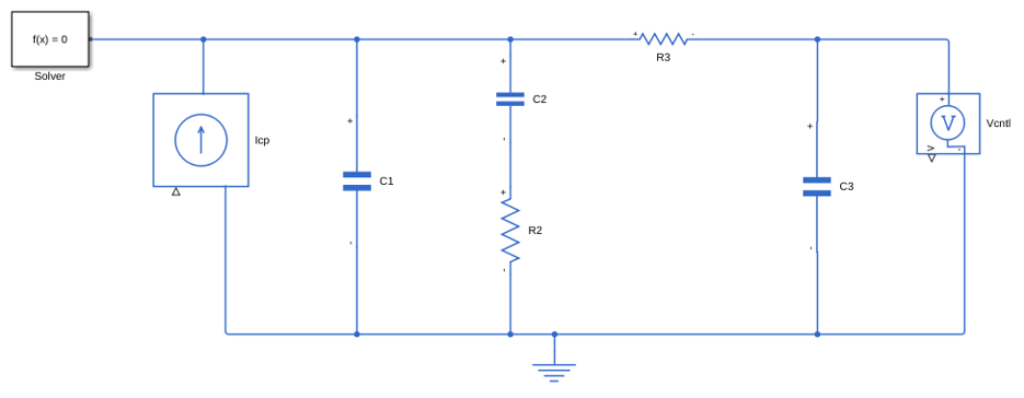
2. Create a circuit configuration object using cktconfig. This parses the Simscape diagram and identifies input ports (Controlled Current Source blocks) and output ports (Voltage Sensor blocks).
cktobj = cktconfig('PllLoopDynamicsCircuit');
3. Enable the device noise generators for the resistors R2 and R3. This adds noise current injection ports at each resistor location, allowing the circuit solver to compute the noise transfer impedance from each resistor to the output.
cktobj.mdlwks.DeviceNoiseGenerators(1).Enabled = 'on';
cktobj.mdlwks.DeviceNoiseGenerators(2).Enabled = 'on';
4. Obtain the state-space model using cktssmodel. The resulting system has three inputs (Icp, R2 noise, R3 noise) and one output (Vcntl). Extract the individual transfer impedances from the MIMO model.
sys_ckt = cktssmodel(cktobj);
zlf_ckt = sys_ckt(1,1);   % Loop filter transfer impedance
zr2_ckt = sys_ckt(1,2);   % R2 noise transfer impedance
zr3_ckt = sys_ckt(1,3);   % R3 noise transfer impedance
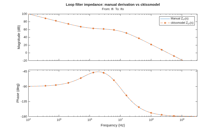
Use a bode plot to demonstrate that the loop filter transfer impedance from cktssmodel is identical to the manually derived model. The noise transfer impedances from cktssmodel include the full circuit response (including integration through C1), which is the correct form for direct use in phase noise calculations.
zlf_ckt.InputName = ''; zlf_ckt.OutputName = '';
figure(7)
bodeplot(zlf, zlf_ckt, opts);
lines = findobj(gcf, 'Type', 'Line');
for i = 1:numel(lines)
    if lines(i).Color(1) > 0.8 && lines(i).Color(2) < 0.5
        lines(i).LineStyle = '--';
        lines(i).Marker = '*';
        lines(i).MarkerIndices = round(linspace(1, numel(lines(i).XData), 15));
    end
end
delete(findobj(gcf, 'Type', 'Legend'));
ax = findobj(gcf, 'Type', 'Axes');
for a = 1:numel(ax)
    if contains(ax(a).YLabel.String, 'Magnitude')
        magLines = findobj(ax(a), 'Type', 'Line');
        legend(ax(a), flipud(magLines), ...
            {'Manual Z_{LF}(s)', 'cktssmodel Z_{LF}(s)'});
        break;
    end
end
title('Loop filter impedance: manual derivation vs cktssmodel');
Z Domain Modeling
This section presents modeling in the uniform sampled time domain (Z domain) as an alternative to modeling in the Laplace domain.
The PFD/CP only samples the phase difference between reference and output once every reference cycle [ 2, 3 ]. Thus the dynamics of the PLL are inherently tied to that uniform sample rate, and the mathematics that rigorously applies to a linear control loop analysis is Z domain mathematics. There are important behaviors such as spurious responses that occur at higher frequencies. However linear mathematics does not apply to those behaviors.
Given a Z domain expression  of the loop filter response, the Z domain expression for the loop gain [ 3 ] is
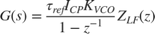
The remaining task is to convert the function from the Laplace domain analysis to the Z domain. There are many ways to perform this task, and several of them have been implemented in the MATLAB c2d function. The appropriate option in this application is zero-order hold, the default for the c2d function. Note that the Z domain modeling does require an explicit sample time value equal to the period of the reference signal.
fref = 30e6;
ts = 1/fref;
vcoz = ss(1,ts*PllKphi*PllKvco,1,0,ts);
divNz = ss(0,0,0,1/PllN,ts);
zlfz = c2d(zlf,ts);
Gz = vcoz*zlfz;

Hz = feedback(Gz,divNz);
Hz.InputName  = 'ref';
Hz.OutputName = 'out';
GzoverN = Gz*divNz;
Compare Z domain with Laplace domain
It is informative to compare the Z domain predictions of the closed loop, open loop, and step responses with the corresponding results from the Laplace domain analysis.
figure(1);
bodeplot(H,Hz,opts);
title('Closed Loop');
legend('Laplace domain','Z domain');

figure(2);
bodeplot(GoverN,GzoverN,opts);
title('Open Loop');
legend('Laplace domain','Z domain');

figure(3);
step(H,Hz);
title('Lock Time');
legend('Laplace domain','Z domain');
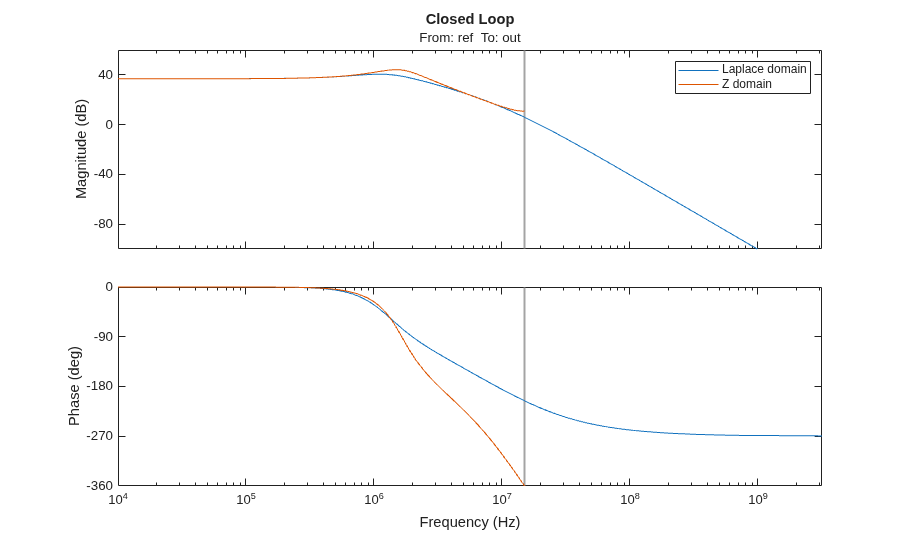
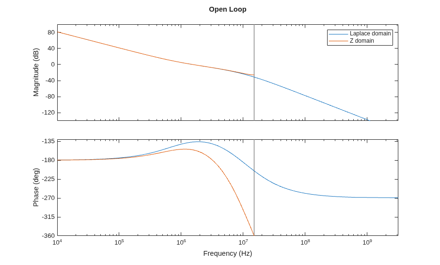
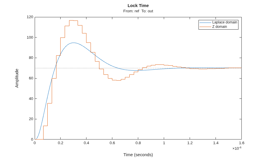
In this comparison, note that while the frequency response and step response from the Z domain analysis are very similar to those obtained from the Laplace domain analysis, the phase margin predicted by the Z domain analysis is far less than the design value chosen as part of the design in the Laplace domain. This is a critical observation, as the loop phase margin is a fundamental requirement of the control loop design.
As stated in [ 2 ], this is a typical result for PLLs whose loop bandwidth equals or exceeds one tenth of the reference frequency. For much smaller loop bandwidths the difference between Z domain and Laplace domain is much smaller.
Note, however, that it is the Laplace domain analysis result that closely matches the time domain simulation. You might find this to be a suitable topic for further study.
Advantages and Disadvantages of Phase Domain Modeling
+ Both open and closed loop linear control analyses are easy, fast, reliable and accurate.
+ You can readily include detailed phase noise modeling in your analysis, with the effect of each phase noise source indicated clearly and accurately.
+ Using the cktconfig and cktssmodel functions, you can easily and accurately include detailed linear circuit designs, especially for the loop filter.
- Phase domain modeling is limited to one sample per reference cycle, and therefore a Nyquist frequency limit of one half the reference frequency. For example, it is not applicable to the analysis of spurious output responses past this Nyquist limit.
- While phase domain modeling can be applied to nonlinear behaviors such as frequency acquisition, such applications lose the inherent advantages of linear control analysis associated with phase domain modeling.
- Phase domain modeling is usually not applicable to models that combine the PLL with other circuits that use the output of the PLL.
References
1. Dean Banerjee, PLL Performance, Simulation and Design, 5th edition, Texas Instruments, SNAA106C, May 2017.
2. P. K. Hanumolu, M. Brownlee, K. Mayaram and Un-Ku Moon, "Analysis of charge-pump phase-locked loops," in IEEE Transactions on Circuits and Systems I: Regular Papers, vol. 51, no. 9, pp. 1665-1674, Sept. 2004, doi: 10.1109/TCSI.2004.834516.
3. Mike Steinberger, "Discrete Time Modeling of PLLs", MathWorks document, May 31, 2022, supporting file attached with this example.

