Eigenmode-Based Solver for PCB Vias
This topic explains the use of an eigenmode-based solver to analyze the return path of a via in a planar structure such as a PCB [1].
You can model the signal path of a via using a lumped element circuit model, but the return current path usually involves structures that are separated from the via by more than a tenth of a wavelength at the maximum frequency of interest (the usual limit for lumped circuit models). This return current path usually involves Ground Return Vias (GRVs) that connect the top and bottom conducting planes in a given PCB layer and can couple with other via signal paths as well.
To model a return path, use radial transverse electromagnetic (TEM) waves that are eigenmodes of the planar structure. You can model the propagation and reflection of these radial TEM waves very accurately, even over very long distances, using closed form linear equations defined at each of the discontinuities in the wave’s propagation path. A matrix solution of these linear equations is used to obtain the return path impedance and signal coupling.
Wave Generation and Propagation
A via cell is a subsection of a via that transitions from one conducting plane, through one or more dielectric layers (possibly containing signal routing) to another conducting plane.
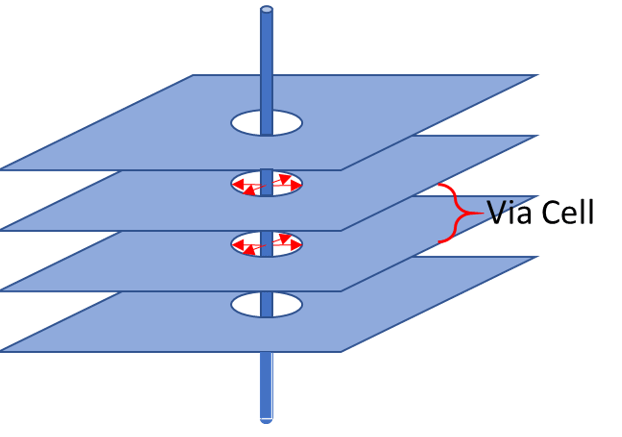
Within a via cell, the signal current flowing along the via barrel is exactly balanced by the return current flowing in the opposite direction across the edge of the antipad.
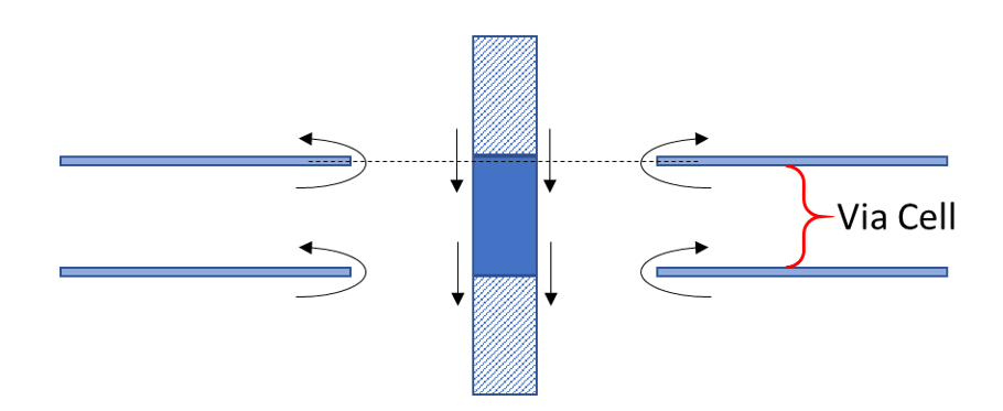
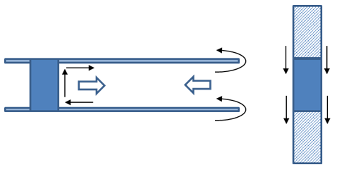
The return current flowing from the edge of the antipad generates a radial TEM wave centered on that via cell. The radial TEM wave propagates outward from the via cell like ripples in a pond. The radial TEM wave creates magnetic coupling between the top and bottom conducting planes, like a half turn transformer. This is one of the mechanisms through which the return current is transferred between the top and bottom planes.
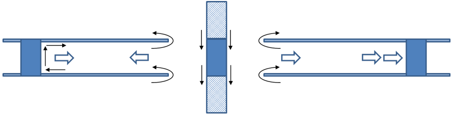
The other current transfer mechanism is a GRV that shorts the top and bottom planes together at some point outside the via cell. A radial TEM wave that is generated at the via cell antipad propagates to a nearby GRV, and is reflected by the GRV, creating another radial TEM wave flowing outward from the GRV.
Radial TEM waves from both the via cell and the GRV on the left continue to propagate, and eventually both waves strike other GRVs, in this case, the waves strike the GRV on the right hand side in the diagram. The waves continue to propagate and reflect, often creating a complex system of waves propagating between the top and bottom planes.
Circuit Model
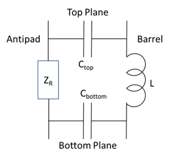
Combine the return path current conduction with the capacitance and inductance between the via barrel and the antipads to produce a complete circuit model for the via cell.
Note
For version one of the via solver feature, the circuit elements Ctop and Cbottom and L in this schematic are automatically calculated to produce a 50-ohm characteristic impedance. There is no modeling of pad capacitances, entry/exit traces, or routing within a layer.
The impedance ZR in the schematic models the circuit behavior of the entire return path and includes any waves reflected from GRVs or the waves propagated from other via cells (crosstalk).
For each layer in a PCB, the equivalent circuits of the via cells are combined into a Generalized Circuit (ABCD) matrix, and the ABCD matrices are combined in series to produce an ABCD matrix for the complete PCB.
Equations and Solutions
This section presents the derivation of the linear matrix equation that the voltages and currents in a given layer must satisfy. This equation is solved for each frequency of interest to obtain the elements of the layer’s ABCD matrix as a function of frequency.
Variables and Functions
| Variable | Name | Descritpion |
|---|---|---|
| Sizes | ||
| n | Via Cells | Number of via cells in the layer |
| m | Radial TEM Waves | Number of radial TEM waves in the layer, m≥n |
| Voltages and Current | ||
| J | Return currents | n✕1 vector of via cell return currents |
| Vout | Outgoing voltage | m✕1 vector of outgoing wave voltages, one for each wave, as measured at the antipads of the via cells and the via barrels of the GRVs |
| Vin | Incoming voltage | m✕1 vector of incoming wave voltages, one for each wave, as measured at the antipads of the via cells and the via barrels of the GRVs |
| Vreturn | Total return voltage | m✕1 vector containing the total return path voltages, as measured at the antipads of the via cells and the via barrels of the GRVs |
| Coefficient Matrices | ||
| B | Generic amplitude | Amplitude coefficient for a zero order outgoing radial TEM wave |
| P | Propagation constants | m✕m matrix of propagation constants between the different via cells and GRVs in the layer |
| Z | Wave output impedances | m✕n matrix of output source impedances for via cell outgoing waves |
| Reflection coefficients | m✕m matrix of reflection coefficients. The reflection coefficients for via cells is zero and the reflection coefficients for GRVs is -1. | |
| Zreturn | Return path impedances | m✕n matrix of impedances for the complete return path response, including reflections and crosstalk. The first rows of this matrix are used to populate the ABCD matrix for the layer. |
| I | Identity matrix | The m✕m identity matrix |
| Speeds and Distances | ||
| k | Propagation constant | is the propagation constant at the frequency of interest. |
| Dielectric impedance | is the impedance of a dielectric | |
| rk | Source radius | Radius at which the outgoing wave voltage is defined – antipad radius for via cells and barrel radius for GRVs |
| Rjk | Propagation distance | Center to center distance between the via cells or GRVs |
| d | Dielectric thickness | The total distance between the top and bottom return planes |
| Functions | ||
| H0(2) | Zero order Hankel function of the second kind | The Hankel function is a combination of Bessel functions for describing the cylindrical geometry of radial TEM waves. A Hankel function of the second kind describes an outgoing wave. A zero order Hankel function describes voltage of a wave that does not vary with azimuth. |
| H1(2) | First order Hankel function of the second kind | The first order Hankel function happens to be the derivative of the zero order Hankel function, and is therefore useful for describing the radial current of a wave that does not vary with azimuth. |
The voltage and current for a zero order radial TEM wave as a function of radius are [2]
The waves from each via cell and GRV propagate to produce incoming waves at the other via cells and GRVs.
In this equation, the propagation constants are approximately
The via solver feature improves the accuracy of this equation by integrating the average around the destination antipad or GRV barrel.
Define the entries in Vout either as being driven by via cell return current or as being the reflection of incoming waves. The general equation is a combination of the two sources.
The mode output impedance Z is the ratio of the TEM wave voltage to current at the edge of the antipad. Each GRV is a nearly perfect short circuit reflector at the edge of its via barrel. If the via cell waves are in rows 1 through n of Vout, then the entries of Z and are
The solution for Vout is
The solution for the complete return path response is
References
[1] Steinberger, Telian, Tsuk, Iyer and Yanamadala, “Proper Ground Via Placement for 40+ Gbps Signaling”, DesignCon 2022, April 2022.
[2] Ramo, Whinnery and Van Duzer, Fields and Waves in Communications Electronics, third edition, section 9.3, John Wiley and Sons Inc., copyright 1994