LTE MIB Recovery and Cell Scanner Using Analog Devices AD9361/AD9364
This example shows how to implement an LTE MIB recovery system partitioned across the processing system (PS) and the programmable logic (PL) of a Xilinx® Zynq® platform with Analog Devices AD9361/AD9364 radio front end. The example demonstrates how to generate HDL IP core for the PL and embedded code for the PS by using HDL Workflow Advisor. The example shows how to run the design on the radio platform and how to reuse the generated FPGA bitstream to build an LTE MIB cell scanner for the detection of LTE cell signals in the local vicinity.
Due to limited hardware resources, this example is not supported on ZedBoard and FMCOMMS2/3/4.
Introduction
The LTE HDL MIB Recovery (Wireless HDL Toolbox) is based on a Simulink® model that you can use to detect MIB information from synthesized data generated with the LTE Toolbox™ or from captured off-the-air LTE waveforms.
This figure shows the hardware architecture diagram of the LTE HDL MIB Recovery example.
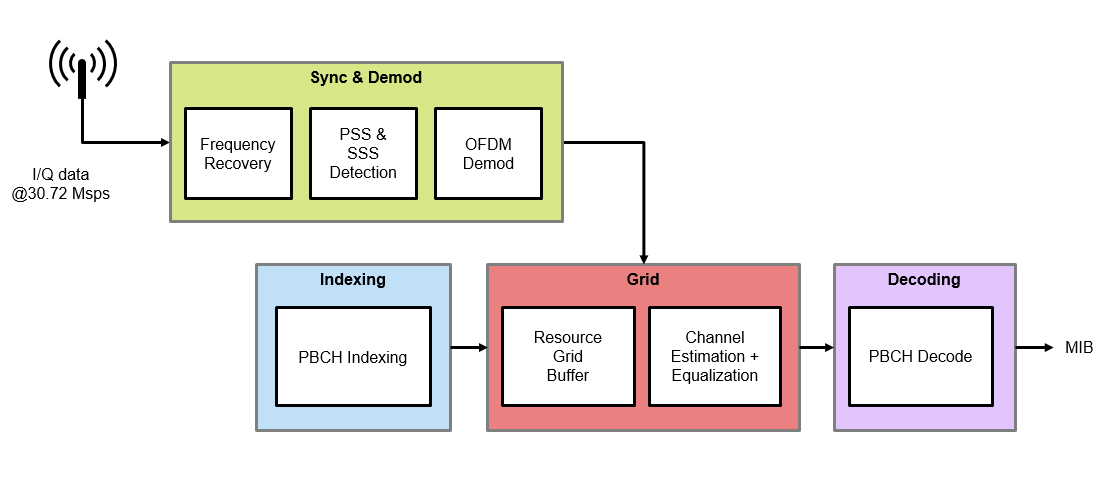
This example adopts the Simulink model from the LTE HDL MIB Recovery example and deploys a hardware-software (HW/SW) co-design implementation of the MIB receiver targeting software-defined radio (SDR). The example demonstrates how to generate an HDL IP core for the PL and embedded code for the PS by using HDL Workflow Advisor. The example shows how to run the MIB receiver design on the radio platform and how to reuse the generated FPGA bitstream to build an LTE MIB cell scanner for the detection of LTE cell signals in the local vicinity.
Setup
To work with the HW/SW co-design workflow, you must install and configure additional support packages and third-party tools. For more information, see Installation for Hardware-Software Co-Design.
Hardware Generation Model
This Simulink model is a hardware generation model of the MIB recovery algorithm. From this model, you can generate HDL code for the PL and generate a template software interface model using HDL Workflow Advisor. Using the template software interface model, you can generate an application that runs on the PS. This diagram highlights the hardware subsystem and the test harness.

HW/SW Partitioning
The LTE_MIB_HDL subsystem contains the functionality to be implemented on the PL. Due to the high rate signal processing requirements of the design, most of the MIB recovery algorithm is implemented on the PL. The ARM processor pulls the information from the FPGA and sends useful information back to the host for display over a UDP link.
The LTE_MIB_HDL subsystem is surrounded by the functionalities to be implemented on the ARM processor as software. These functionalities include:
Correcting any coarse frequency offset
Starting and resetting control of the HDL IP
Sending the decoded MIB information to the host for display.
Controlling which input data to use: off-the-air or pregenerated test data stored on the FPGA.
To simulate software execution on the hardware, the output data of the subsystem is downsampled by 1000.
LTE_MIB_HDL Subsystem
The LTE_MIB_HDL subsystem adopts the LTE Cell Search and MIB Recovery model from the LTE HDL MIB Recovery (Wireless HDL Toolbox) example and adds additional functionality to integrate the model with the Zynq hardware architecture.

This figure shows the HDL LTE MIB Recovery subsystem from the LTE HDL MIB Recovery (Wireless HDL Toolbox) example. For more details on this subsystem, see the HDL Optimized LTE MIB Recovery section of the example.
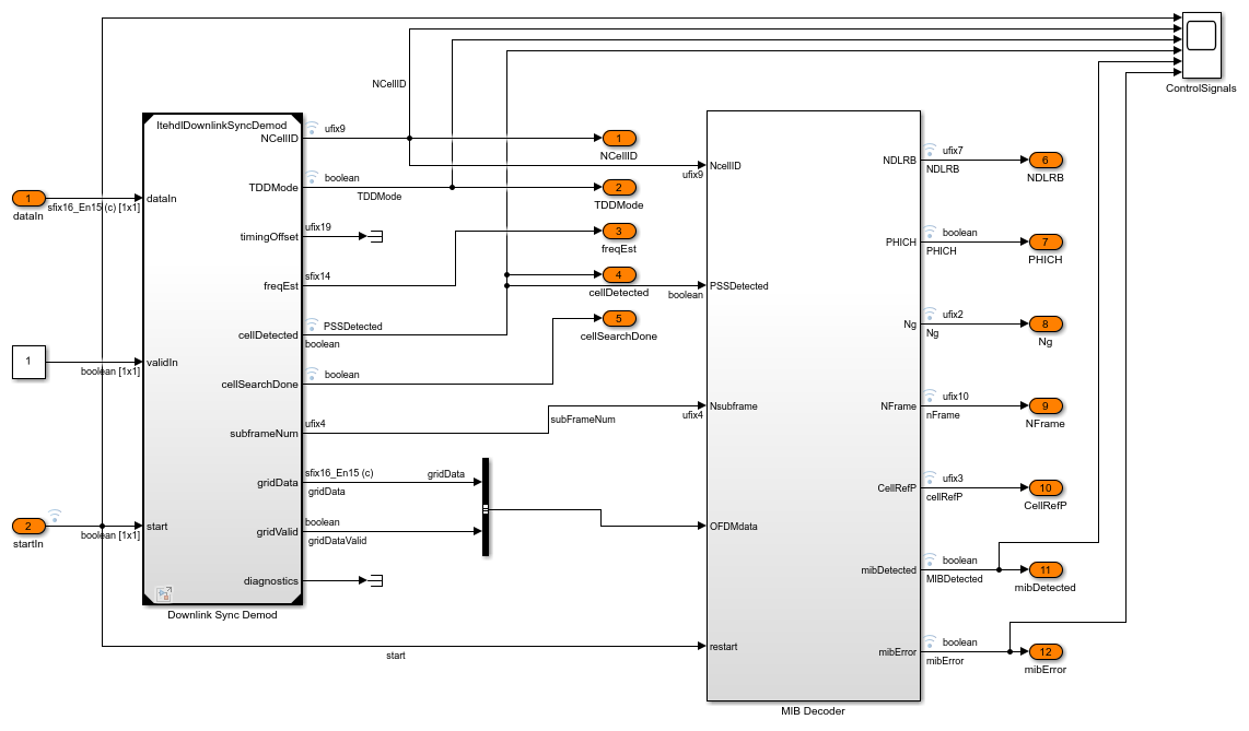
The StimulusSelector selects the input data to the MIB recovery algorithm by switching between off-the-air waveform or test data. The test data is pregenerated using LTE Toolbox and stored in a lookup table on the FPGA.
The PrepInputs subsystem adjusts the rate and format of the received data. The data received from the ADC of the AD9361/AD9364 RF chip is a 12-bit value, sign-extended to 16 bits. To use the full range, the StimulusSelector subsystem scales the data samples to 16 bits. To take advantage of hardware resource sharing and to simplify the receiver architecture, the StimulusSelector subsystem also configures the data rate. The input data rate is 61.44 MHz, whereas the required maximum data rate is 30.72 MHz. This difference translates to an overclocking factor of  . Therefore, the StimulusSelector subsystem downsamples the data by a factor of 2. An FIR Decimation block implements a lowpass decimation filter which captures the central part of the received LTE waveform and downsamples the data to 30.72 MHz.
Simulate Hardware Generation Model
To confirm its operation, you can run the hardware generation model by using the LTE waveforms stored in the zynqRadioLTETransmitData.mat file. The zynqRadioHWSWLTEMIBDetectorInit initialization script configures the waveforms used in the model. As the model contains a large number of HDL-optimized blocks which require simulation using sample-based signals, the simulation may take a while. Once the MIB is decoded, the example displays the decoded information.
To use the internal test data transmitted from a lookup table (LUT), set the value of the externalDataSel block to false. In this case, the model drives the start signal internally, resetting the MIB recovery every 4s.
To select precaptured off-the-air data stored in the test vectors, set the value of the externalDataSel block to true.
Once you are satisfied with the simulation behavior of the hardware subsystem, you can start the process of generating the HDL IP Core, integrating it with the SDR reference design, and generating software for the ARM processor.
Generate IP Core
In preparation for targeting, you must set up the Xilinx tool chain by invoking the hdlsetuptoolpath function. For example:
>> hdlsetuptoolpath('ToolName','Xilinx Vivado','ToolPath','C:\Xilinx\Vivado\2019.1\bin\vivado.bat');
Start the targeting workflow by right-clicking the LTE_MIB_HDL subsystem and selecting HDL Code > HDL Workflow Advisor.
In Step 1.1, select the
IP Core Generationworkflow and the appropriate Zynq radio platform:ADI RF SOM,ZC706 and FMCOMMS2/3/4,ZCU102 and FMCOMMS2/3/4, orZC706 and FMCOMMS5. Due to limited hardware resources, this example does not support ZedBoard and FMCOMMS2/3/4.In Step 1.2, select receive path reference design. For this example, you can use default reference design parameters.
In Step 1.3, the interface table maps the DUT signals to the interface signals available in the reference design. Because this example uses a single channel, configure the channel 1 connections and AXI register interfaces as shown in these images.

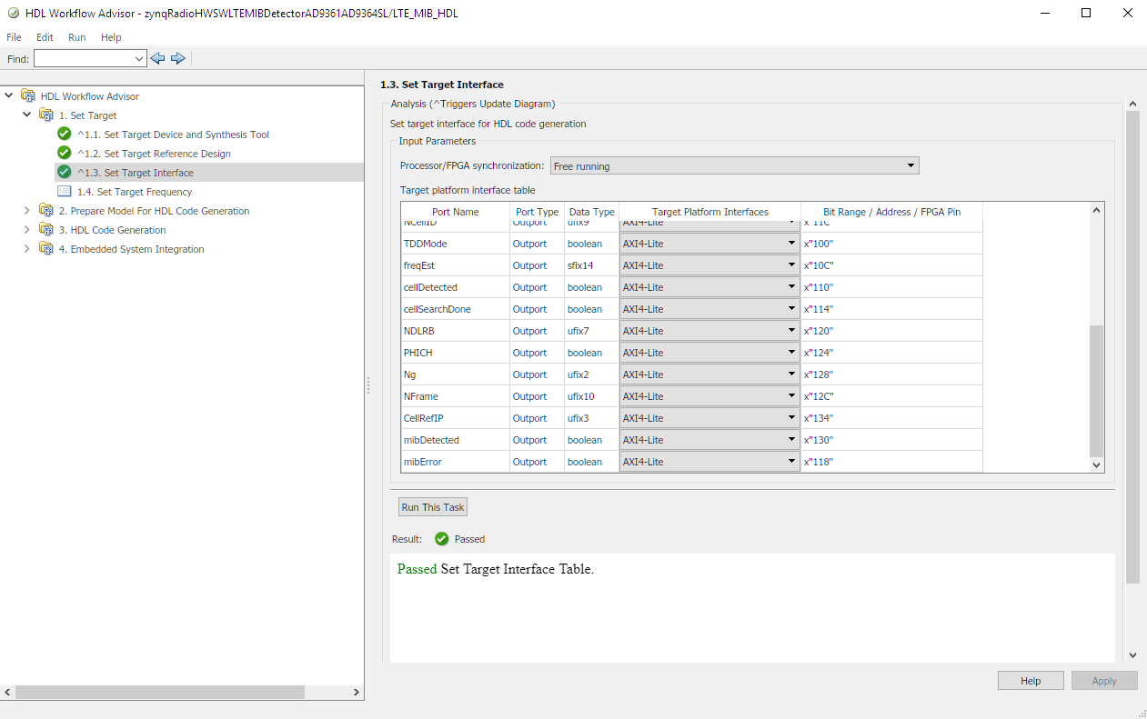
In Step 1.4, set the DUT synthesis frequency. The DUT synthesis frequency depends on the baseband sampling rate of the system. For this example, you can use the default sampling rate value of 61.44 MHz.
Step 2 prepares the model for HDL code generation by performing design checks.
Step 3 generates HDL code for the IP core.
Generate Software Interface Model and Block Library
Step 4 of the HDL Workflow Advisor integrates the newly generated IP core into the Zynq SDR reference design, generates the corresponding bitstream, and loads the bitstream onto the board.
Step 4.2 generates a software interface library and a template software interface model.
Software Interface Library
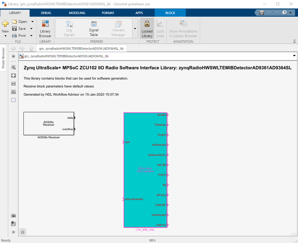
The library contains the AXI Interface block generated from the LTE_MIB_HDL subsystem and an AD936x Data Read block. The data ports of the receiver block represent the streaming data interface between the FPGA user logic and the ARM processor. Because the hardware generation model does not contain any SDR receiver blocks, the AD936x Data Read block parameters are set with default values.
When using the library blocks in a model, you must configure the parameters correctly for your application. Take into account that any updates to the LTE_MIB_HDL subsystem are automatically propagated to the library blocks in the model when you run Step 4.2 again.
Template Software Interface Model

You can use the generated template software interface model as a starting point for a full SW targeting, such as, external mode simulation, processor-in-the-loop, and full deployment. Because the generated model is overwritten each time you run Step 4.2, it is recommended to save this model under a unique name and develop your software algorithm there.
Generate and Load Bitstream
The last steps of the HDL Workflow Advisor generate a bitstream for the PL and download the bitstream onto the board.
Step 4.3 generates a bitstream for the PL. You can execute this step in an external shell by selecting Run build process externally. This selection allows you to continue using MATLAB while building the FPGA image. Once some basic project checks are complete, Step 4.3 is marked with a green checkmark. However, you must wait until the external shell displays a successful bitstream build before moving on to the next step.
Step 4.4 downloads the bitstream onto the device. Before continuing with this step, make sure that MATLAB is set up with the correct physical IP address of the radio hardware by calling the
zynqfunction.
>> devzynq = zynq('linux','192.168.3.2','root','root','/tmp');
By default, the physical IP address of the radio hardware is 192.168.3.2. If you alter the radio hardware IP address during the hardware setup process, you must supply that address instead.
Alternatively, if you want to load the bitstream outside Workflow Advisor, create an SDR radio object and use the downloadImage function. The radio object to create depends on the radio platform selected in Step 1.1.
If the selected radio platform is either
ADI RF SOMZ,ZC706 and FMCOMMS2/3/4, orZCU102 and FMCOMMS2/3/4, create an AD936x radio object.
>> radio = sdrdev('AD936x');
If the selected radio platform is
ZC706 and FMCOMMS5, create an FMCOMMS5 radio object.
>> radio = sdrdev('FMCOMMS5');
Download the bitstream using the radio object interfacing the selected radio device.
>> downloadImage(radio,'FPGAImage', ...
     'hdl_prj\vivado_ip_prj\vivado_prj.runs\impl_1\system_top.bit')
     % Path to the generated bitstream
LTE MIB Recovery Software Interface Model
The LTE MIB Recovery model is developed from the generated template software interface model. The model attempts to detect cells and decode MIBs at the specified center frequency. The Reset and Coarse Frequency Search Controller block corrects the frequency offset up to 22.5 kHz by stepping through potential offsets. The search stops when an optimal step is found which results in MIB decoding with minimal corrected fine frequency offset. The Restart Controller block resets the cell search and MIB decoding in the HDL IP either upon MIB detection or when the detection times out. The Restart Controller block also communicates with the Coarse Frequency Search Controller and calibrates the center frequency before the MIB decoding. When running with internal test data, a much simpler state machine is used as there will be no frequency offsets.
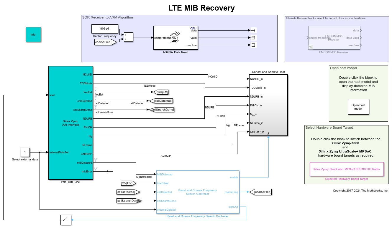
The model is configured for the Xilinx Zynq-7000 Based Board target. You can use this target for the ADI RF SOM, ZC706 and FMCOMMS2/3/4, or ZCU102 and FMCOMMS2/3/4 radio platforms. For the ZCU102 and FMCOMMS2/3/4 radio platform, you must reconfigure the model by selecting Zynq UltraScale+ MPSoC ZCU102 IIO Radio in Model Settings (Ctrl+E) > Hardware Implementation > Hardware board. You can also do this by double clicking the Selected Hardware Board Target block.
Run Design on Zynq Board
You can run the LTE MIB Recovery software interface model in Monitor & Tune mode. In this mode, you can control the configuration from the Simulink model. Alternatively, to deploy the design on the board disconnected from Simulink, click Build Deploy & Start.
Set the source of the LTE MIB detection:
To use the waveform stored on the FPGA, set the input to the
externalDataSelblock to 0.To detect a live off-the-air signal, set the input to the
externalDataSelblock to 1. This option requires the transmission center frequency of an LTE cell tower in your area. The default center frequency for this example is 806 MHz.
The software algorithm is configured to reset the receiver on a timeout with a default value of 1000, which corresponds to 1 second. The hardware start signal is configured to reset the receive every 4 seconds.
Host Interface Model
The ARM sends the decoded MIB information directly back to the host over the Ethernet link using the UDP send block. The IP address of the UDP send block must be the IP address of the host, by default, '192.168.3.1'. If you altered the IP address during the hardware setup process, you should supply that address instead.
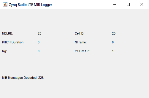
This interface model running on the host receives the UDP data sent by the Zynq Radio, unpacks the data, and displays the data in real time using the scope block. The following UDP receive model illustrates how to receive the decoded data, and displays the result.

When running successfully, the example displays the data received from the test waveform on the FPGA.
LTE MIB Cell Scanner SW Interface Model
Using the hardware generation model, you can also implement an LTE MIB cell scanner. To scan across center frequencies and search for LTE cell towers in the local vicinity, you can reuse the FPGA bitstream generated for the MIB detector example. You only need to modify the LTE MIB Recovery software interface model by updating the center frequency over time and to check for valid MIB signals, as shown in the LTE MIB Cell Scanner model. You can also run this model in Monitor & Tune mode or can fully deploy the model on the board.

The AXI Interface block reads and writes registers on the MIB detector IP core. The ARM-FPGA interface block configures RF parameters. You can tune the center frequency in real-time from the software algorithm. To select the band of the scan, set the parameters in the LTE Cell Scanner and Coarse Frequency Search Controller block.
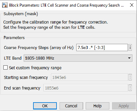
The LTE Cell Scanner and Coarse Frequency Search Controller block uses a MATLAB state machine. The state machine programs the center frequency, gives the RF card time to settle, and waits for valid MIB signals. The numMIBRetries port determines the number of MIB detections on each center frequency.
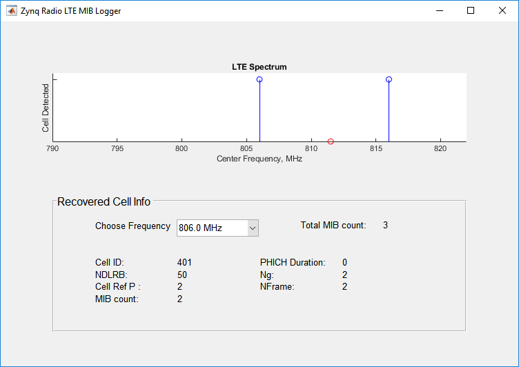
The Concat and Send to Host block sends the MIB information and associated data packages to the host over the UDP. To enable the host display model to update its state periodically, the block also sends the current center frequency to the host at regular intervals.
To view the decoded MIB information, open the LTE MIB Logger host model. This model display the MIB information and the center frequency of the current scanning.
Summary
This example shows how to implement an LTE MIB detector and an LTE cell scanner deployed as a HW/SW co-design implementation using the same hardware generation model. The generated HDL IP core suits both implementations. The generated software interface model serves as a template that can accommodate the development of control-specific aspects of each algorithm apart.
See Also
AD936x Data Read | AD936x Data Write