Software and Task Management on Processor
The processor system in this SoC application reads data from the external memory following a write from the FPGA to that memory. Since FPGA writes and interaction with external memory are asynchronous, the processor uses an event-driven task to read from memory. The software also manages a register on the FPGA that specifies a multiplication factor to be used in the FPGA algorithm.
Processor Model
Open a new Simulink® model. Save the model as
soc_hwsw_proc.slxinto a new subfolder, namedprocessor, in the project folder. Add thesoc_hwsw_proc.slxmodel to the project.In Simulink, configure the
soc_hwsw_top.slxmodel to as an SoC application. On the Apps tab, under Setup to Run on Hardware, click System on Chip (SoC).In the System on Chip (SoC) pop-up window, select Hardware Board > Xilinx Zynq ZC706 evaluation kit. Click Finish.
Note
The processor model must use the same hardware board and solver configuration parameter settings as the top level model.
In the Configuration parameters window, in the Hardware Implementation panel, set Processing Unit to
APU.In the model, using a Function-Call Subsystem block, Asynchronous Task Specification (Simulink Coder) block, Inport block, and Outport blocks, create the following system.
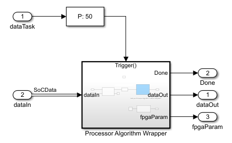
In the
dataTaskblock dialog mask, check Signal Attributes > Output function call to expose a function call port on the outside model.In the Asynchronous Task Specification block dialog mask, set Task priority to
50.Note
The task priority of the Asynchronous Task Specification block must match the priority of task in the Task Manager block driving this task.
Task Processing
The Processor Algorithm Wrapper subsystem reads data from the
external memory only after each write to the external memory by the FPGA.
Open the
Processor Algorithm Wrapperblock.Using a Stream Read block, Constant block, Data Type Conversion block, and Subsystem blocks, create the following model.
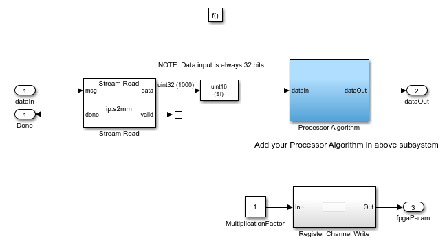
Open the Stream Read block dialog mask. Set Number of buffers to
6.Open the Data Type Conversion block dialog mask and set Output data type to
uint16.The
Processor Algorithmsubsystem serves as a base to develop your own processing algorithm.Open the
Register Channel Writesubsystem block.Add a Register Write block to create the following model.

Open the Register Write block dialog mask. Set Device name to
/dev/mwsinewavegenerator_ip0and Offset address tohex2dec('100').
Top Model
In the project folder, open the model
soc_hwsw_top.slx.Add a Subsystem block into the
Processorarea and label the blockProcessor.In the
Processorsubsystem, using the Task Manager block and Model block, create the following system.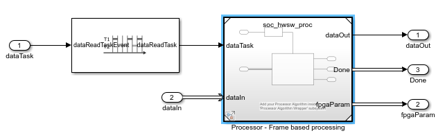
Open the Model block dialog mask and set Model name to
soc_hwsw_proc.slx.Open the Task Manager block dialog mask. Set the task Name to
dataReadTaskand set the Priority to50. In the Simulation tab, set the Mean, Min, and Max to8e-05. Click OK.