HW/SW Co-Design Implementation of ADS-B Receiver Using Analog Devices AD9361/AD9364
This example shows how to implement algorithms on the Zynq radio platform that are partitioned across the ARM and the FPGA fabric. Specifically, this example concerns the reception and decoding of Automatic Dependent Surveillance Broadcast (ADS-B) transmissions, with receive functionality implemented in hardware and software, and a transmit waveform embedded in hardware.
Introduction
This example involves the reception of ADS-B transmissions either from the air, or from a previously recorded Mode S signal which can be transmitted locally using the embedded transmit waveform. The transmit and receive FPGA implementations are combined into one HDL IP core and implemented on the Zynq programmable logic (PL). The data decoding is run on the Zynq ARM processor through code generation. Some control parameters are added to the FPGA IP core to show how the design can be adjusted in the real time using AXI4-Lite registers accessed from Simulink.
Setup
If you have not already done so, ensure you follow the Installation for Hardware-Software Co-Design in the documentation.
Mode S Messages
Mode S is a transponder interrogation mode used to transmit information about an aircraft upon request from an interrogating system. Mode S signals can be either short (56 bits) or long (112 bits). The content of different Mode S message types can vary significantly, all of them will contain information regarding the message type, the ICAO24 identification address of the aircraft, and a cyclic redundancy check (CRC) checksum. For this example, consider Mode S Extended Squitter (Mode S ES) transmissions, which are 112 bit signals that can contain additional information about the altitude, position, velocity, flight status, and callsign of an aircraft. this figure shows the structure of a typical Mode S ES signal.

The initial eight bits of any Mode S signal are the control bits. These bits contain information on the downlink format (DF), which is used to describe which type of Mode S message is being received. For Mode S ES, the value of the DF must be equal to 17. This is followed by the ICAO24 code, which is a unique 24-bit aircraft identification code. The additional 56 bits of information included in a Mode S ES Signal make up what is known as the ADS-B message.
The content of an ADS-B message is identified through its Type Code (TC), which is the first 5 bits of the message. Depending on the type code, an ADS-B message can contain information about the aircraft ID (TC=4), airborne position in terms of altitude, latitude and longitude (TC=9), and horizontal and vertical velocity (TC=19). This example is specifically concerned with the decoding of airborne position messages, which are structured as shown in the diagram below.

Mode S signals are preceded by an 8-bit preamble pattern, which is used by receivers to determine if a valid message has been transmitted, and when the message bits start. The signals are transmitted at 1090 MHz at a data rate of 1 Mbit/s, and are modulated using Pulse Position Modulation (PPM), as illustrated in the following figure.

For PPM, a Logic 1 is obtained when the signal is ON for the first half of a bit interval and OFF for the second half. Likewise, a Logic 0 is obtained when the signal is OFF for the first half of a bit interval, and ON for the second half. As PPM Modulation is extremely time sensitive, it is important that a Mode S receiver is able to use the preamble to determine the exact sample where the message bits start.
Hardware Generation Model
You can use the hardware generation model to develop the functionality that you want to implement on the FPGA fabric. This involves modelling an HDL-optimized ADS-B receiver for implementation onto the PL. In this example, we transmit and repeat on a single board (through the use of the embedded transmit waveform), however, you can modify the example to receive ADS-B signals from the air. You can do this by changing the receive center frequency from the default 2.4GHz value to 1090 MHz, and disabling the transmitter blocks.
![]()
Hardware Software Partitioning: In general, the programmable logic of the FPGA is used for high rate signal processing while the ARM is used for slower rate, control functionality. In this example, the receiver algorithm is implemented entirely in the PL, as the matched filtering and cyclic redundancy checks (CRC) introduce high rate signal processing requirements. The embedded transmit waveform is also implemented in the PL. The Tx and Rx algorithms have been placed in two separate subsystems - HDLTxIpCore and HDLRxIpCore - within the main HDL_ADSB subsystem. The ARM is used to send the received data back to the host for decoding and printing.
This model contains an AXI4-lite control port, TxTransmitPeriod. This allows control over the rate at which ADS-B messages are transmitted. The Threshold port sets the minimum received amplitude required to register a correctly received preamble. This figure shows the transmit subsystem.
![]()
The pre-recorded ADS-B extended squitter messages are stored in a 2-D Lookup Table block, where each column contains 512 samples. The first HDL Counter block counts to the value specified by the TxTransmitPeriod port. Once the period value is reached the first timer resets while in the same instance incrementing the second timer, which selects the next column to read from. The second timer resets every eight periods, for the eight stored extended squitter messages. The model is configured to allow a transmit period of up to 4s to be used.
The receive algorithm, shown below, uses a discrete FIR filter block to correlate the received data to the preamble. The Timing Control state machine then uses the correlation value to trigger reception of data.
![]()
The timing control state machine in this example has been implemented in MATLAB code using a MATLAB function block. The preamble is detected if a peak with amplitude greater than the threshold value is output from the FIR filter. The threshold value is calculated dynamically using an estimate of the received signal power. Once the preamble has been located, the state machine waits for the start of the first message bit before triggering the processing of a message.
Within the Bit Process subsystem, the amplitude of the samples for the first and second halves of the bit period are calculated and compared in order to determine whether the current bit is Logic 1 or Logic 0. This can be considered a form of PPM demodulation. A HDL counter is also used within this subsystem in order to determine the starting point of each new bit, based on the 4 MHz sampling rate of the system. The output of this counter is used to compute a CRC checksum within the Compute and Check CRC subsystem, which will then be compared to the received checksum in order to ensure that the received ADS-B message is valid. In order for this comparison to take place, the timing control state machine empties the CRC registers for the final 24 bits of the received message. This is achieved by setting the EmptyReg signal appropriately.
At the output, the received and processed data is delayed by the length of one long Mode S signal and converted into a 16-bit integer for ease of decoding. A message is decoded using some MATLAB code if the valid output is at Logic 1.
This model can be run to confirm its operation using the embedded transmit waveform within the HDLTxIpCore subsystem. When you run the model, the received messages are decoded and presented on a table GUI.
IP Core Generation Workflow
If the simulation behavior of the hardware subsystem is as expected, you can start the process of generating the HDL IP Core, integrating it with the SDR reference design, and generating software to run on the ARM.
In preparation for targeting, you must set up the Xilinx tool chain by invoking hdlsetuptoolpath. For example:
>> hdlsetuptoolpath('ToolName','Xilinx Vivado','ToolPath','C:\Xilinx\Vivado\2019.1\bin\vivado.bat');
Start the targeting workflow by right-clicking the HDL_ADSB subsystem and selecting HDL Code / HDL Workflow Advisor.
In Step 1.1, select
IP Core Generationworkflow and the appropriate Zynq radio platform from the choices: ADI RF SOM, ZC706 and FMCOMMS2/3/4, ZedBoard and FMCOMMS2/3/4, ZCU102 and FMCOMMS2/3/4, ZC706 and FMCOMMS5.
In Step 1.2, select
Receive and transmit pathreference design. You can leave the reference design parameters as defaults.
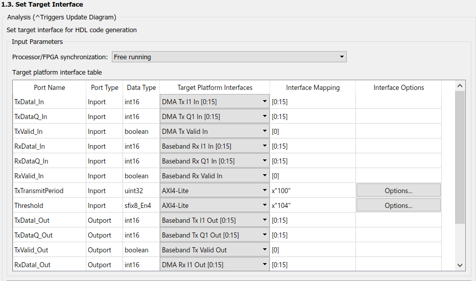
In Step 1.3, In Step 1.3, use the interface table to map the user logic signals to the interface signals available in the reference design. In this example, use a single channel, so that you can connect the channel connections to the relevant ports as shown below.


In Step 1.4, ensure that the Target Frequency is set to a reasonable number given the baseband sampling rate of the system. In this example, the sample rate is 4 MHz, so a synthesis frequency of around 8 MHz is more than sufficient.
Step 2 prepares the model for HDL code generation by doing some design checks.
Step 3 performs the actual HDL code generation for the IP core.
Step 4 integrates the newly generated IP core into the larger Zynq SDR reference design, generates the bitstream and helps you load it onto the board.
Execute each step in sequence to experience the full workflow, or, if you are already familiar with preparation and HDL code generation phases, right click Step 4.1 in the table of contents on the left hand side and select Run to selected task.
Software Generation Model and Block Library
In Step 4.2, the workflow generates a Zynq software generation interface model and a block library. Click the
Run this taskbutton with the default settings.
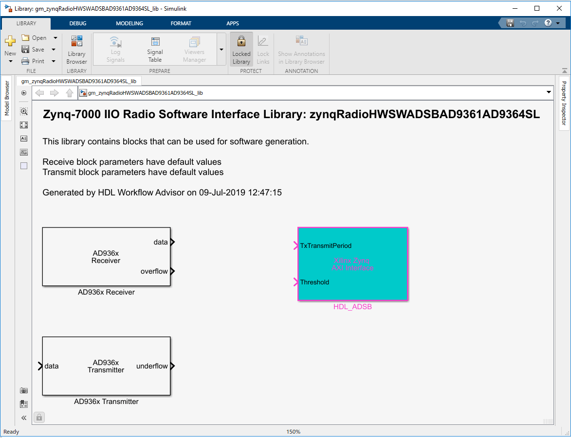
Software Interface Library

The library contains the AXI Interface block which has been generated from the HDL_ADSB subsystem. Note that this exposes only the AXI4-lite control ports, and not the data ports. The data ports are present on the Receiver/Transmitter blocks which represent the data interface between the FPGA user logic and the ARM. If you use the library blocks in your downstream models, any updates you make to your HDL subsystem will automatically be propagated to this library and then to your software generation models when you run through the workflow. In this example, the hardware generation model did not contain any SDR transmit or receive blocks so the parameters on these blocks could not be populated. When using the library blocks you must ensure to configure the parameters correctly for your application.
Software Interface Model

The software interface model can be used as a starting point for full SW targeting to the Zynq: External mode simulation, Processor-in-the-loop and full deployment. Note that this generated model will be overwritten each time Step 4.2 is run, so it is advisable to save this model under a unique name and develop your software algorithm in there. A software interface model has been provided which shows how you may decide to structure this model, see section Running the Software and Hardware on the Zynq board.
Bitstream Generation and Loading
The rest of the workflow is used to generate a bitstream for the FPGA fabric and download it to the board.
In Step 4.3, the workflow advisor generates a bitstream for the FPGA fabric. You can choose to execute this step in an external shell by ticking the selection
Run build process externally. This selection allows you to continue using MATLAB while the FPGA image is being built. The step will complete in a couple of minutes after some basic project checks have been completed, and the step will be marked with a green checkmark. However, you must wait until the external shell shows a successful bitstream build before moving on to the next step.
Step 4.4 downloads the bitstream onto the device. Before continuing with this step, call the
zynqfunction with the following syntax to make sure that MATLAB is set up with the correct physical IP address of the radio hardware.
>> devzynq = zynq('linux','192.168.3.2','root','root','/tmp');
By default, the physical IP address of the radio hardware is 192.168.3.2. If you alter the radio hardware IP address during the hardware setup process, you must supply that address instead.
Alternatively, if you want to load the bitstream outside Workflow Advisor, create an SDR radio object and call the downloadImage function on the object.
If in step 1.1 you selected either the ADI RF SOM, the ZC706 and FMCOMMS2/3/4, the ZedBoard and FMCOMMS2/3/4, or the ZCU102 and FMCOMMS2/3/4 radio device, create an AD936x radio object.
>> radio = sdrdev('AD936x');
If in step1.1 you selected the ZC706 and FMCOMMS5 radio device, create an FMCOMMS5 radio object.
>> radio = sdrdev('FMCOMMS5');
Download the bitstream using radio object interfacing the selected radio device.
>> downloadImage(radio,'FPGAImage', ...
     'hdl_prj\vivado_ip_prj\vivado_prj.runs\impl_1\system_top.bit')
     % Path to the generated bitstream
Running Software and Hardware on Zynq board
A software interface model has been provided that shows how you could modify the generated model to set it up for the ADS-B Mode S example. This interface model will allow you to run the model in Monitor & Tune mode or fully deployed.
Note that the Transmitter block still has a data input. Even though no data is being sent from the ARM to the FPGA, this block is required to initialize the required RF parameters and to enable the transmit data path, therefore it must be included in the interface model.
![]()
The model has been configured to run using the Xilinx Zynq-7000 Based Board target for the following hardware: ADI RF SOM ZedBoard and FMCOMMS2/3/4 ZC706 and FMCOMMS2/3/4/5
If you are using the ZCU102 and FMCOMMS2/3/4, double click the Selected Hardware Board Target block to change the configuration to use the Xilinx Zynq UltraScale+ MPSoC ZCU102 IIO Radio board target.
The model has been configured to run from a timer-driven scheduler. The downstream decode and display processing will take place when a valid waveform has been received, controlled by the data valid output. If no valid ADS-B signal is received, the attempt to receive data from the FPGA will time out.
In order to successfully receive an ADS-B signal with this example, you can run in one of two ways:
Detect a live signal off-the-air. For this option you will need to set the center frequency of the receiver block to the ADS-B transmission frequency, which is 1090 MHz. You should also comment out the transmitter block to ensure no interfering signal is transmitted.
Use the provided embedded transmit waveform. In this case, the centre frequency of the transmit block should be set to a frequency that is unlicensed and legal to use in your area, with the receiver block set to the same center frequency.
Monitor & Tune mode allows you to control the configuration from the Simulink model. You can also fully deploy the design to run on the board, disconnected from Simulink. In the Simulink toolbar, click Build, Deploy & Start. In this mode you will not be able to tune parameters.
Once the ARM has successfully received a ADS-B message, it sends the result back to the host over the Ethernet link using the UDP Send block found in the software interface model. The UDP Send block has been configured using the default IP address of the host '192.168.3.1'. If you altered the IP addresses during the hardware setup process, you must supply that address instead. A simple UDP receive model has been supplied which has a MATLAB function block used to decode the received messages.
![]()
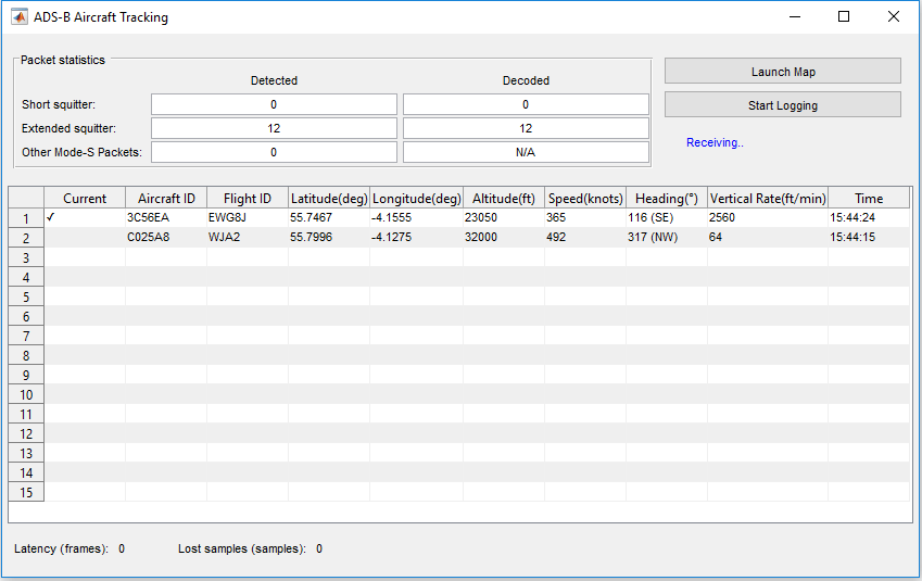
Click Start Logging button to present the decoded information on a tabular GUI or to log detailed information into a text file. If you want to observe the plane traffic in your area, tune your receiver on the interface model to 1090 MHz.

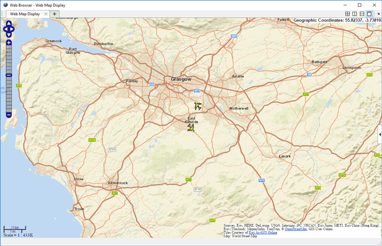
Additionally, if you have a valid license for the Mapping Toolbox™, you can observe the planes on a map. The recorded waveform that comes with this example contains eight captured ADS-B extended squitter messages of two different flights. For each flight there are two airborne position (TC=9), 1 aircraft ID (TC=4) and 1 vertical velocity (TC=19) messages that are repeatedly transmitted at a rate regulated by the TxTransmitPeriod control port.

See Also
AD936x Data Read | AD936x Data Write