Model Simscape Synchronous Buck Converter for Real-Time Simulation and Deployment
This example shows how to model a synchronous buck converter by using Simscape™ switches and dynamic switches. You can generate HDL code and deploy onto a target hardware.
Set Up Synthesis Tool Path
To synthesize the generated HDL code, before you use HDL Coder™ to generate code, set up your synthesis tool path. For example, if your synthesis tool is Xilinx® Vivado®, install the latest version of Xilinx Vivado as shown in HDL Language Support and Supported Third-Party Tools and Hardware.
Then, set the tool path to the installed Xilinx Vivado executable by using the hdlsetuptoolpath function:
hdlsetuptoolpath('ToolName','Xilinx Vivado','ToolPath','C:\Xilinx\Vivado\2022.1\bin\vivado.bat')
Synchronous Buck Converter
A synchronous buck converter topology is a modified version of the basic buck converter circuit topology in which the freewheeling diode is replaced by an insulated gate bipolar transistor (IGBT). It is widely used for efficient power conversion applications such as in portable devices, computing systems, telecommunications, and automotive electronics. The synchronous buck converter contains two power IGBTs with anti-parallel diodes, an output inductor, and an output capacitor. This allows bidirectional power transfer. It produces a regulated voltage lower than its input voltage and delivers high currents with minimum power losses.
Model Synchronous Buck Converter by Using Simscape Switches
This example shows the topology of a DC-DC synchronous buck converter with a sample time of 20 ns. The switches are triggered by a 100 kHz pulse with a duty cycle, D, of 0.25. The voltage at the output is stepped down by the duty cycle. The output voltage, Vout, is calculated as Vin*D.
Open the model at the MATLAB® command prompt.
open_system("sschdlexSynchronousBuckConverterExample");

The configurations inside the FPGA Subsystem block run on an FPGA board and the components that are outside the FPGA Subsystem block run on a CPU in real time. Open the FPGA Subsystem block that contains Simscape blocks.
open_system("sschdlexSynchronousBuckConverterExample/FPGA Subsystem")
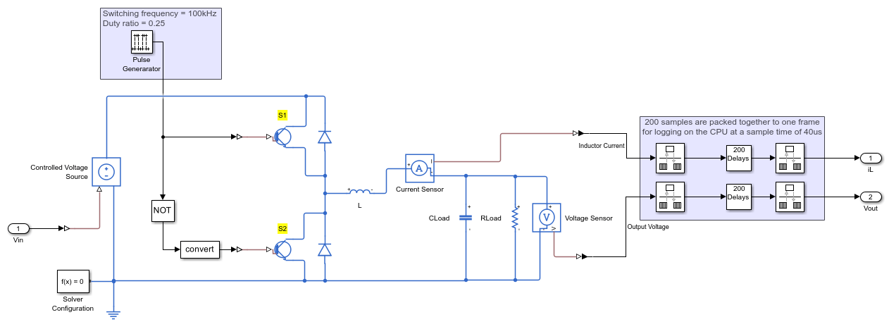
The FPGA Subsystem block contains the Pulse Generator block and synchronous buck converter circuit. You can generate VHDL code for the blocks inside this FPGA Subsystem block.
Note: The model runs at a sample time of 20 ns. The CPU cannot handle such a small sample time,consider downsampling the sample time to 200 ns and packing 200 samples to one frame to log the output signals on the CPU at a rate of 40 μs.
Run Desktop Simulation
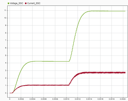
The input to the synchronous buck converter model is an input voltage step wave ranging from 20 V to 48 V. The input signals (that include a PWM frequency and duty cycle) are generated in the FPGA Subsystem block of the model with the sample time of the Simscape model set to 20 ns. You can simulate the model and see the waveforms. The scope provides the output voltage and inductor current waveforms. Alternatively, you can double-click the Data Logger on top of the output signals and open the Simulation Data Inspector.
Generate HDL Code and Synthesize the Results
To generate the HDL code, first generate an HDL implementation model from the Simscape model by using the Simscape HDL Workflow Advisor. For details, see Generate Optimized HDL Implementation Model from Simscape.
After the task passes in the Advisor, you see a link to the generated HDL implementation model. You generate HDL code for this generated HDL implementation model and synthesize the HDL code. For details about the HDL code generation and synthesis of code, see Generate FPGA Bitstream for Two-Phase DC-DC Converter with Tunable Run-Time Parameters.
You can select the data type precision in the Generate implementation model task pane of the Simscape HDL Workflow Advisor.
The synchronous buck converter model is synthesized for two cases:
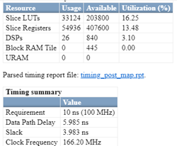
Case1 — Data type precision is set to Single and an equivalent state-space model is generated with a Validation logic tolerance of 2e-2.
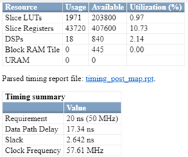
Case2 — Data type precision is set to Fixed-point with Fixed-point word length set to 32-bit. The equivalent state-space model is generated with a Validation logic tolerance of 2e-2.
Model Synchronous Buck Converter by Using Dynamic Switches
You can generate an optimized model for the FPGA deployment by replacing the Simscape switches with their dynamic equivalents from the SimscapeFPGAHIL_lib library. To optimize the model, run the sschdl.generateOptimizedModel function at the MATLAB command prompt:
generatedModel = sschdl.generateOptimizedModel("sschdlexSynchronousBuckConverterExample");
An optimized model is generated for the synchronous buck converter model and is saved as sschdlexSynchronousBuckConverterExample_generated. In this model, the FPGA Subsystem block contains the replaced blocks.
The desktop simulation results for the synchronous buck converter, modeled with dynamic switches shows similar waveforms when the converter is modeled by using Simscape switches. For the output voltage and inductor current waveforms, refer to the previous section.
Generate HDL Code and Synthesize the Results
You can generate HDL code for the generated optimized model and synthesize the HDL code as directed in previous section.
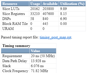
You can select the data type precision in the Generate implementation model task pane of the Advisor. The optimized synchronous buck converter model is synthesized for two cases:
Case1 — Data type precision is set to Single and an equivalent state-space model is generated with a Validation logic tolerance of 2e-3.
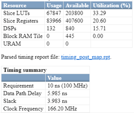
Case2 — Data type precision is set to Fixed-point with Fixed-point word length set to 32-bit. The equivalent state-space model is generated with a Validation logic tolerance of 2e-2.
Deploy Synchronous Buck Converter to Speedgoat FPGA I/O Modules
You first run the HDL Workflow Advisor to generate RTL code and IP core, create a Vivado project, and build the FPGA bitstream. Then, deploy the generated bitstream onto a Speedgoat IO334-325k module.
Generate FPGA Bitstream for Speedgoat Target Computer
For the PCIe Interface, all the input and output ports of the FPGA Subsystem block must be of either data type single or fixed-point with word lengths up to 32 bits. If they are not, add a Data Type Conversion block at each input and output port.
1. Open the HDL implementation model, and then open the HDL Workflow Advisor for the implementation model.
open_system("gmStateSpaceHDL_sschdlexSynchronousB")
To open the HDL Workflow Advisor for a subsystem inside the model, use the hdladvisor function.
hdladvisor("gmStateSpaceHDL_sschdlexSynchronousB/FPGA Subsystem")
2. In the Set Target Device and Synthesis Tool task, specify Target workflow as Simulink Real-Time FPGA I/O and Target platform as Speedgoat IO334-325K.
3. In the Set Target Reference Design task, select a value of X4 for the parameter PCIe lanes, and click the Run This Task button.
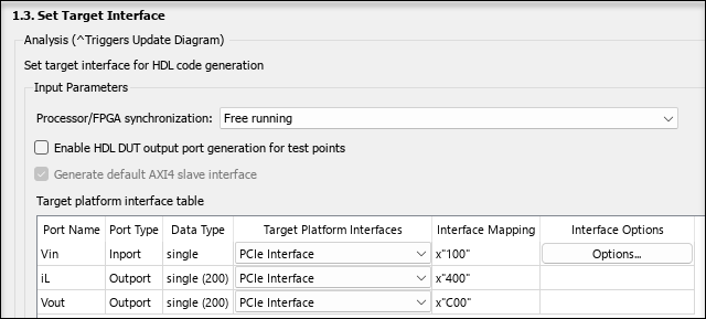
4. In Set Target Interface task, map the input and output single data type ports to PCIe Interface and click the Run This Task button.
5. In the Set Target Frequency task, the default value of Target Frequency (MHz) is set to 100. For this example model, this value is 50.
6. Right-click the Generate Simulink Real-Time Interface task, and select Run to Selected Task to generate the HDL IP core and FPGA bitstream.
Deploy Bitstream to Speedgoat IO334-325k Target
The FPGA Subsystem is automatically replaced in the real-time interface model with Speedgoat® driver blocks to initialize the hardware and to interface with the FPGA during run time.
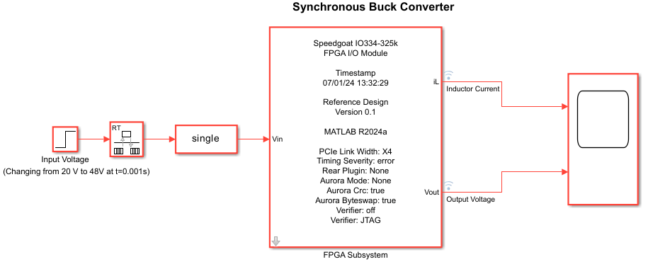
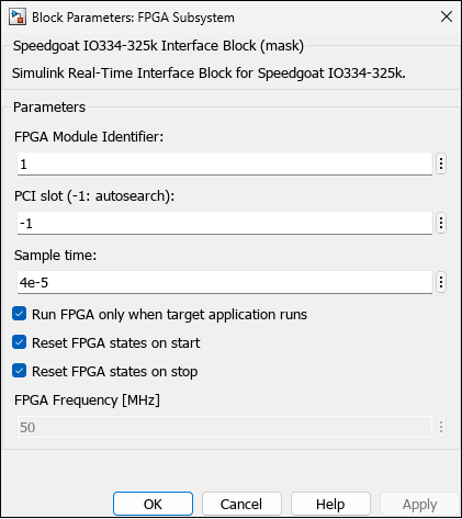
For the FPGA Subsystem block, change the Sample time parameter to 4e-5. All the inputs to the FPGA Subsystem block must run at 4e-5. Therefore, a Rate Transition block is inserted.
Connect to Target Machine and Run Real-Time Simulation
The model can now be deployed onto the Speedgoat real-time target machine.
1. Make sure that the Speedgoat real-time target machine is connected to the host computer and powered on.
2. Download the bitstream by using the Simulink Real-Time Explorer. To open the Simulink Real-Time Explorer, enter the command slrtExplorer. Alternatively, you can open the Explorer from the Real-Time tab of the Simulink Toolstrip.
3. The Simulink Editor displays the Real-Time tab for models that are configured for the speedgoat.tlc code generation target. Click the Connect to Target Computer button in the Simulink Real-Time tab to connect to the machine. Once connected, click the Run on Target button to deploy the model.
4. Simulink Real-Time™ automatically generates C code from your model by using Simulink Coder™. The generated code and the bitstream for the FPGA are loaded onto the target machine, and model execution starts automatically.
See Also
sschdl.generateOptimizedModel | sschdladvisor | hdladvisor