Logic Timing Simulation
This example shows how to use the Variable Pulse Delay block to create accurate timing models of logic circuits.
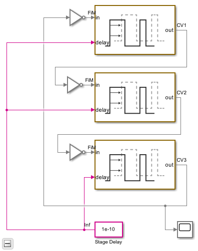
The delays in this model are introduced by the Variable Pulse Delay blocks from the Utilities library of the Mixed-Signal Blockset™, with the delay defined by a separate input to the block. The initial output values for the Variable Pulse Delay blocks are set to guarantee oscillation. The initial output values for two of the blocks are kept at the default value of zero while the initial output for the third block is set to one.
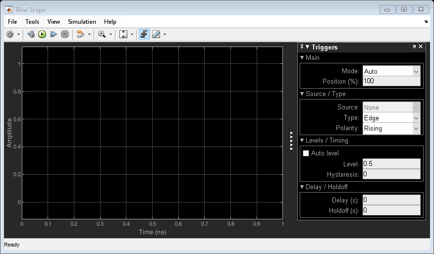
The oscilloscope is configured to display the samples as a scatter graph, with no rendering between samples. Different sample times make different assumptions about the signal value between samples such as:
Zero Order Hold (ZOH) — The signal value is assumed to equal the value of the most recent sample.
First Order Hold (FOH) — The signal value is assumed to vary linearly from one sample to the next.
Nyquist limited — The signal is assumed to have zero spectral content above a frequency equal to one half of a fixed sample rate.
Taylor series — For each major sample step, an ODE solver produces a polynomial that approximates the signal value over that time interval.
The oscilloscope block bases its rendering on these assumptions. You must focus on the samples themselves and understand explicitly the assumptions that different sample times make.
The samples displayed on the oscilloscope show a single sample for each logic switching event. These samples are generated by the Variable Pulse Delay blocks. Every time a Variable Pulse Delay block receives a sample, it generates a new event at a time equal to the sample time plus the value at the delay input port.
As indicated by the sample time color coding, the output sample time for the inverters is Fixed In Minor Step (FIM). This means that each inverter produces an output sample value for every major sample time in the model, regardless whether or not that sample time is used at an input port of the gate.
This FIM behavior is typical of most logic blocks; however you should pay special attention to sample time propagation in triggered subsystems such as D flip-flops. If the trigger input uses a fixed step discrete sample time, then any input which is not synchronous with that sample time may not be processed correctly. The triggered subsystem can be forced to operate in FIM mode by triggering it with a variable step discrete trigger such as would be produced by the Variable Pulse Delay block or the Logic Decision.
Since the model does not contain any differential equations, the solver is Variable Step Discrete.
The Stage Delay is set to 100 ps, resulting in a half period of precisely 300 ps and a period of 600 ps, as demonstrated in the simulation output.
Load the logic timing model and update the model to display sample times.
open_system('LogicTiming');
set_param(gcs,'SimulationCommand','update');
Run the logic timing model.
%%.
sim('LogicTiming');