Model Continuous-Time Band-Pass Delta-Sigma Modulator
This example shows different ways of implementing a continuous-time (CT) band-pass delta-sigma modulator (BP-DSM) based on multi-path feedback loop or using a Finite Impulse Response (FIR) filter in the feedback path.
This example describes a step-by-step procedure to synthesize the architecture, set the main simulation parameters, select the model topology, simulate the model and get main performance metrics. This example uses Cascade of Resonators with Feedback (CRFB) architecture for the DSM using and order.
Design Flow
To design a delta-sigma modulator, typically you start the process by defining the noise transfer function (NTF) of a given topology. The NTF is chosen for the sake of the performance, and it can be expressed as [1][2]:
where stands for the transfer function of the feedback path of a discrete-time (DT) DSM, and can be easily obtained by using Richard Schrier's Delta-Sigma Toolbox [3]. To this end, specifications used in this example are:
Modulator order (
L): L=2 for -order modulators or L=4 for -order modulators.Oversampling ratio (
OSR) = 64Optimize zeros (
opt) = 0 (a flag used to request optimized NTF zeros).Maximum out-of-band gain of the NTF (
H_inf) = 1.5Center frequency of the modulator (
f0) = 0.25 (it sets the center [notch] frequency at 0.25 of the sampling frequency).
ntf = synthesizeNTF(2, 64, 0, 1.5, 0.25);           % Synthesize the NTF [3] (L=2 as example)
L1_z = 1/ntf-1;                                     % Definition of L1(z) as a function of NTF
The code above considers a -order modulator. This example also proposes -order topology using multi-path feedback loops and FIR filter in the feedback loop based on IEEE paper On the Use of FIR Feedback in Bandpass Delta-Sigma Modulators [4].
The Simulink® representations of the Bandpass DSMs (BP-DSM) which use multi-path feedback and FIR filter are shown below. You need multi-path feedback to set a direct mapping between DT and CT resonators. As explained in [4], use of FIR filters significantly reduce out-of-band quantization error in the feedback signal, thus making CT DSMs more robust in terms of linearity and clock jitter.
Multi-Path Feedback Loop in -Order CRFB CT BP-DSM
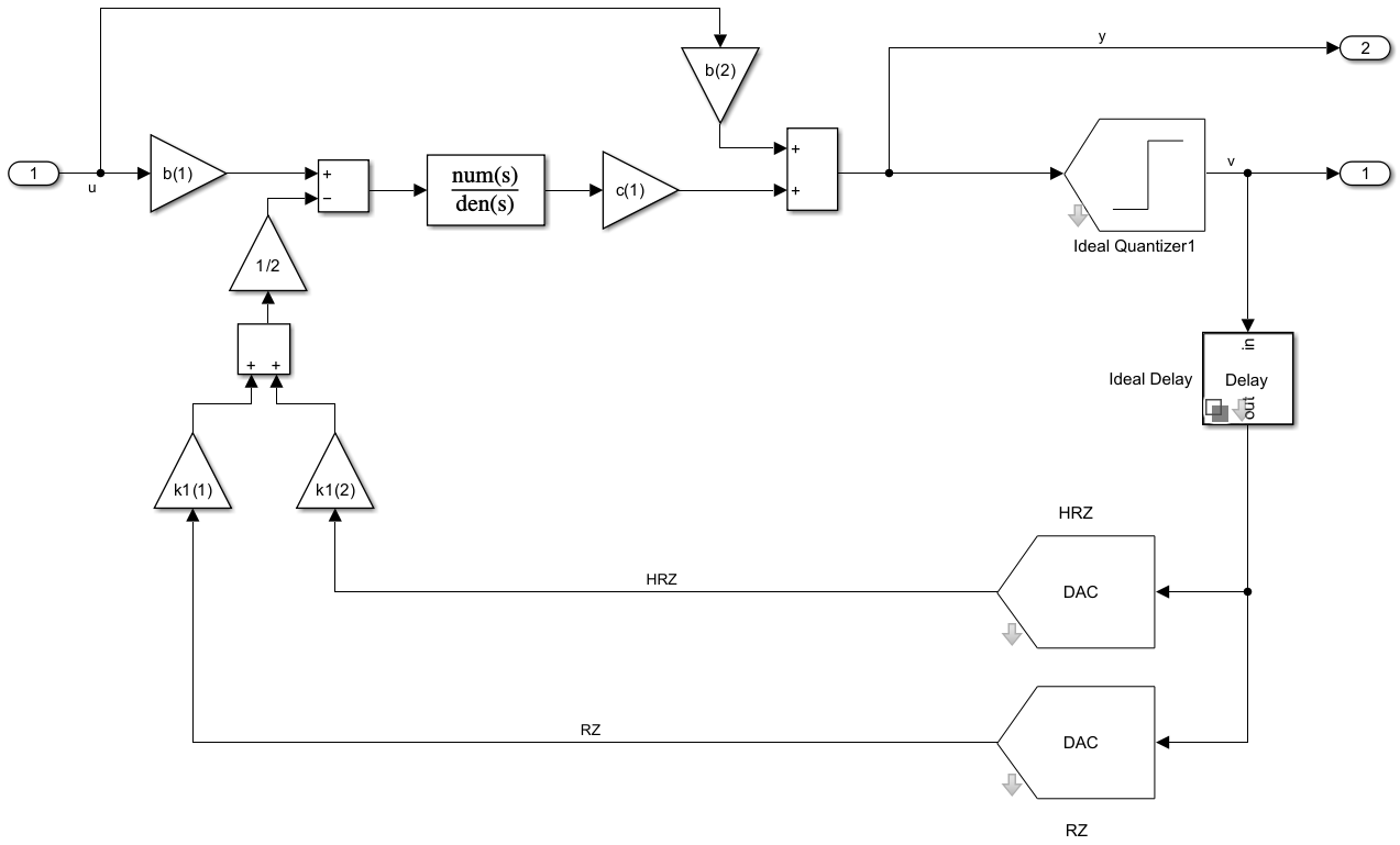
Multi-Path Feedback loop in -Order CRFB CT BP-DSM

FIR Filter in -Order CRFB CT BP-DSM

FIR Filter in -order CRFB CT BP-DSM

Once you obtain the NTF of the DT DSM, the next step is to apply Impulse-invariant Transformation (IIT) to obtain the loop-filter coefficients of the equivalent continuous-time (CT) DSM. There are several methods to perform IIT, among which the example uses the modified Z-transformation methodology [1][2]. The loop-filter coefficients required for each topology in the example model is already set, since the comprehension of IIT is beyond the scope of this example.
model =1; % model selection open_system('ord_2nd_4th_CRFB_CT_BP_all_models.slx');
Design parameters shared by the four models are listed below:
Sampling frequency (
fs) = 128 kHzBandwidth (
Bw) = 1e3 kHz (obtained as Bw=fs/(2*OSR))Notch frequency (
fn) = 32 kHz (center frequency of the band-pass filter, obtained as fn=fs/4)Input signal amplitude (
A) = 0.5 VInput signal frequency (
fin) = 32990 kHzResonance frequency of resonators () = rad/s
Gain of resonators () = rads
Number of points for the FFT (
N) =
Another point to note is that every model considers a delay of 1 sample period in its feedback path in order to compensate the effect of excess loop delay (ELD).
Evaluate DSM Performance
Here is the screenshot of the testbench used to evaluate the performance of the DSM

Once a modulator topology has been selected, you can proceed to simulate it.
out = sim('ord_2nd_4th_CRFB_CT_BP_all_models.slx');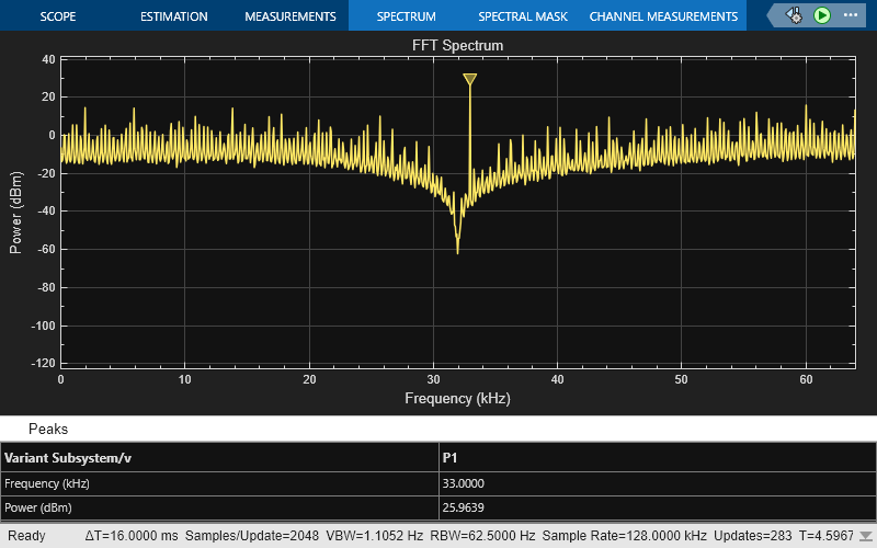
The spectrum analyzer used in the model depicts the FFT spectrum of the output signal. It illustrates how the quantization noise is shaped so that it is pushed out of the band of interest.
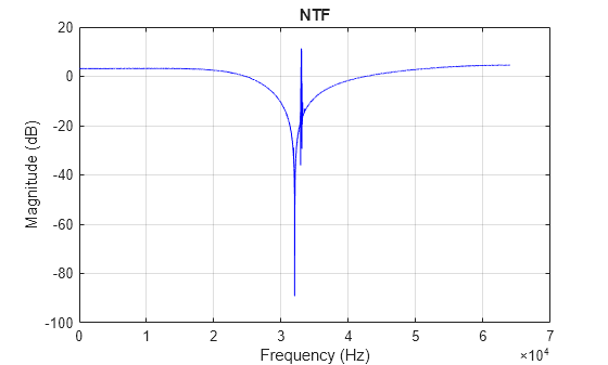
The simulation also returns the values of the input signal (U), the output of the modulator (V), and the signal at the input of the quantizer (Y) to the workspace. You can plot the NTF by processing the data as follows:
N = 2^14;                                                   % FFT points
fs = 128e3;                                                 % sampling frequency
f = (1:N/2)*(fs/N);                                         % frequency array
w = hanning(N);                                             % window to apply over the processed signals
specV = 20*log10(2*abs(fft(out.v.*w))/sum(w));              % FFT spectrum of V
specVY = 20*log10(2*abs(fft((out.v-out.y).*w))/sum(w));     % FFT spectrum of V-Y
specNTF = specV-specVY;                                     % shape of the NTF

figure('Name','NTF');
plot(f, specNTF(1:N/2), 'b');
title('NTF'); xlabel('Frequency (Hz)'); ylabel('Magnitude (dB)');
grid on;
In the example model, the simulation shifts the output signal to base band. You can also observe that in the model the shifted signal feeds an FIR decimator which filters the out-of-band noise and decimates the output of the DSM. This processed signal allows us to use ADC AC Measurement block from Mixed-Signal Blockset™ in order to evaluate figures of merit, such as signal-to-noise ratio (SNR) and effective number of bits (ENOB):
FoM = table(adc_ac_out.SNR, adc_ac_out.ENOB, 'VariableNames',{'SNR', 'ENOB'});
disp(FoM);
     SNR       ENOB
    ______    ______

    42.378    6.7472
Comparing the results obtained from all 4 cases, you can observe an expected pattern where resolution of the DSMs increase with the loop filter order. You can clearly see a jump in ENOB by ~ 1 bit when moving from 2nd order to a 4th order loop filter. Additionally, when you compare results from two different realization of filters (i.e. FIR based and multi-path feedback based,) you can see the same resolution as long as the filter order remains same. Note that in the case of the FIR, you can observe small differences in the results which will depend on the number of taps in the FIR.
Conclusion
This example shows how to model, simulate and obtain the FFT spectrum and NTF representation of four unscaled band-pass Delta Sigma Modulators. Two different modulator topologies and orders have been proposed to be compared. The simulation results point out that the resolution of DSMs depend on the filter order, the oversampling ratio and also to some extent on the loop-filter realization [4].
References
[1] Shanthi Pavan; Richard Schreier; Gabor C. Temes, Understanding Delta-Sigma Data Converters, Wiley-IEEE Press, second edition, copyright 2017.
[2] Jose M. de la Rosa, Sigma-Delta Converters: Practical Design Guide, Wiley-IEEE Press, second edition, copyright 2018.
[3] Richard Schreier (2022). Delta Sigma Toolbox (https://www.mathworks.com/matlabcentral/fileexchange/19-delta-sigma-toolbox), MATLAB Central File Exchange. Retrieved June 14, 2022.
[4] J. Gorji, S. Pavan and J.M. de la Rosa: “On the use of FIR Feedback in Bandpass Delta-Sigma Modulators.” IEEE Trans. on Circuits and Systems -- I: Regular Papers, vol. 71, No. 3, pp. 1082-1092, March 2024. DOI: 10.1109/TCSI.2023.3336719.
[6] G. Molina-Salgado, A. Morgado, G. Jovanovic Dolecek and J.M. de la Rosa: “LC-based Bandpass Continuous-Time Sigma-Delta Modulators with Widely Tunable Notch Frequency,” IEEE Trans. on Circuits and Systems -- I: Regular Papers, vol. 61, No. 5, pp. 1442-1455, May 2024. DOI: 10.1109/TCSI.2013.2289412.
See Also
Continuous Time Delta Sigma Modulator