Architectural 112G PAM4 ADC-Based SerDes Model
This example shows how to use a IEEE 802.3ck specification transmitter and receiver architectural model using library blocks in the SerDes Toolbox™ library and custom blocks to model a 112G PAM4 time-interleaved ADC-based SerDes. The performance impact of the timing mismatch between the time-interleaved ADCs is explored as an example of a design trade-off study. The aspects of the model which are compatible with the IBIS-AMI 7.0 standard are used to create an IBIS-AMI model.
Overview
There are many tradeoffs to be explored when designing an ADC-based SerDes. Some of these design trade-offs and resulting questions are summarized below:
ADC Exploration
What type of ADC will be used in this design? Flash, binary/multibit search, or SAR (successive approximation register)?
What ADC time-interleave factor should be used? What is the impact on system performance caused by mismatches of the timing, gain, voltage offset and/or bandwidth between parallel ADCs and explore mismatch calibration algorithms?
What full-scale range should be used?
What resolution/quantization/number of bits is required?
Should the quantization be uniform or non-uniform?
What is the performance impact of quantization noise?
Digital Equalization Exploration
What number of FFE taps is required to achieve needed performance?
How many DFE taps can be implemented?
What DSP resolution is required?
What impact does frame size or parallelism of digital processing have on system latency. What demultiplexer width should be used?
Clock Recovery
What bandwidth of CDR is required? How should the loop filter be specified?
Which Mueller-muller cost function is best for the application?
Analog Front End
How many CTLE stages are needed?
How does the CTLE amplified noise impact system performance?
How to scale signals in order to take advantage of the linear range of the ADC?
This example focuses on determining the impact of the time-interleaved timing mismatch between parallel ADCs. The model can be the basis of exploring many other design tradeoffs. The system SNR (signal-to-noise ratio) is compared between cases with and without a 4% symbol time timing offset and shows that this impairment reduces the system performance by about 2.5 dB.
Rx Model Description
The receiver model is composed of an analog front-end (AFE) with CTLE and amplifier blocks. The time-interleaved ADC is further parallelized by a demultiplexer before DSP processing by the FFE and DFE. The baud-rate CDR controls the VCO which drives the ADC. The system performance is quantified by a SNR metric as well as an output waveform. This model is summarized in the following diagram where the time-interleave depth (or the number of ADC's) is four and the demux size is 64.
Open the Simulink® model ArchitecturalADCBasesSerDes.slx attached with this example.

The receiver analog front-end partially equalizes the waveform and is very similar to the ADC IBIS-AMI Model Based on COM. Here the first block injects the input referred noise, followed by the mid-band zero CTLE, main CTLE, and noise filter CTLE blocks as specified by channel operating margin (COM) of IEEE 802.3ck. The VGA scales the signal to match the full scale range of the ADC and the Saturating Amplifier block enforces a memoryless-nonlinearity.

ADC Subsystem
The ADC subsystem is composed of custom ADC, Demux, RxFFE, DFE, Phase Detector, Loop Filter, and VCO System object™ blocks. Additionally, the IBIS-Bridge and IBIS-AMI clock_times blocks facilitate the conversion of the model to an IBIS-AMI model.

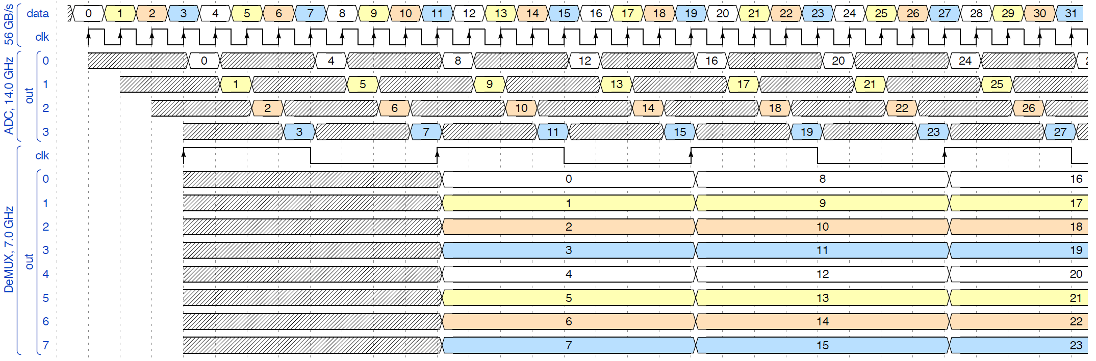
A time-interleaved ADC is utilized to reduce the maximum speed and latency requirements of a full-rate ADC. The diagram below shows how four time-interleaved ADCs can take turns sampling the data signal.

The sampled signals are demuxed or framed to reduce the signaling rate before processing with the DSP equalization. The diagram below illustrates how a demux width of 8 frames slows down and parallelizes the data. The model itself is parameterized to use a demux of 64 but 8 are shown below for illustration purposes only.
Next a 21 tap FFE is applied to the parallelized signal and is then followed by the single tap DFE and data decision. The baud-rate phase detector utilizes a type A Mueller-Muller phase detector that aims to balance the ISI of the first pre- and post-cursor samples as illustrated below:

The phase detector output is processed with the loop filter which in turn drives the voltage controlled oscillator (VCO) or the heart-beat of the system. This VCO drives the other blocks and closes the system loop.
SNR Calculation
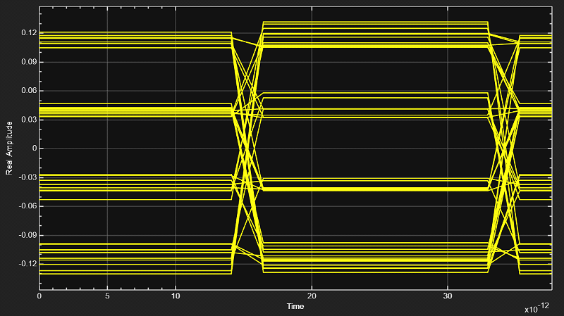
For ADC-based serdes the eye diagram is not as information rich as it is for analog SerDes. Instead signal-to-noise (SNR) calculations and vertical eye slices are more useful insight into the system performance.
The DFE block calculates the SNR as follows:
where is the signal strength and is the noise strength. If represents the discrete equalized sampled voltages, then for NRZ the signal and noise strengths are defined as,
For PAM4, the signal and noise are defined in terms of the middle and outer sampled symbol voltages.
The histogram plot shows the clustering of the four PAM4 symbols.

FFE and DFE Equalization Adaptation
Very similar to the process used in the ADC IBIS-AMI Model Based on COM example, the FFE and DFE tap adaptation is performed in AMI Init at time 0 with impulse-response based analysis in the initialize subsystem. These optimized tap values are then passed to the Simulink equalization blocks and are utilized throughout the simulation.
Impact of Timing Mismatch
If the phases of the several clocks that drive the time-interleaved ADCs are not equally spaced from each other, then system performance degradation occurs. While much of this timing mismatch can be calibrated out, it is important to understand the performance impact of this impairment. The RxClock or the VCO block has a parameter called the Max Timing Mismatch (UI). This parameter injects a phase offset between the first and second clocks. While this is a simplistic model of actual system behavior, it is sufficient to illustrate the impact.
If you have not done so yet, open the Simulink model ArchitecturalADCBasesSerDes.slx attached with this example.
Run the model and observe the baseline behavior. When the simulation completes, the Simulation Data Inspector automatically loads up the logged signals.
Double click on the Rx Clock/VCO block and change the timing mismatch to be 0.04 and re-run the model. The resulting SNR for the two runs can be compared as follows. This illustrates how a small 4% timing mismatch can reduce the system performance by about 4.5 dB.

Generate ADC-Based SerDes IBIS-AMI Model
The final part of this example takes the customized ADC-based SerDes Simulink model and then generates an IBIS-AMI compliant model including model executables, IBIS, and AMI files.
The current IBIS AMI standard does not have native support for ADC-based SerDes. The current standard is written for slicer-based SerDes, which contain a signal node wherein the equalized signal waveform is observed. In a slicer-based SerDes this node exists inside the DFE, right before the decision sampler. A continuous analog waveform is observable at that node, which includes the effect of all the upstream equalizers (such as CTLE) and the equalization due to DFE, as tap weighted and fed back prior decisions. Such a summing node does not exist in an ADC-based SerDes, due to the ADC in the system. In a real ADC-based SerDes system the ADC proves a vertical slice though the eye at the sampling instant. To emulate a virtual node, the IBIS-AMI Bridge block reassembles the discrete equalized samples according to the time interleave factor and the demux size. A single equalized sample is held constant for the entire IBIS-AMI waveform symbol time.
Export IBIS-AMI Models
Open the Export tab in the SerDes IBIS-AMI manager dialog box.
Verify that Dual model is selected for both the Tx and the Rx AMI Model Settings. This will create model executables that support both statistical (Init) and time domain (GetWave) analysis.
Set the Tx model Bits to ignore value to 5 since there are three taps in the Tx FFE.
Set the Rx model Bits to ignore value to 20,000 to allow sufficient time for the Rx DFE taps to settle during time domain simulations.
Set Models to export as Both Tx and Rx so that all the files are selected to be generated (IBIS file, AMI files and DLL files).
Press the Export button to generate models in the Target directory.
Explore Further
The number of ADCs and the Demux width in the model is parameterized by the MATLAB® workspace variables timeInterleaveDepth and DemuxSize. They are set in the model PreLoadFcn callback and can be changed to other positive integers as part of further exploration. The system objects in the ADC subsystem can be modified to explore many of the design tradeoff questions identified at the first of the example.
References
[1] S. Kiran, S. Cai, Y. Zhu, S. Hoyos and S. Palermo, "Digital Equalization With ADC-Based Receivers: Two Important Roles Played by Digital Signal Processingin Designing Analog-to-Digital-Converter-Based Wireline Communication Receivers," in IEEE Microwave Magazine, vol. 20, no. 5, pp. 62-79, May 2019, doi: 10.1109/MMM.2019.2898025.