Non-Linear CTLE Modeling
This example shows how to create a behavioral model of a receiver composed of a nonlinear CTLE (or peaking filter) equalizer circuit where the only insight into the circuit is the input versus output behavior. High-speed interconnects like Ethernet and PCIe continue to increase in data rate to support the ever-growing digital bandwidth needs. The need to create fast behavioral models of the receiver equalization is a necessary abstraction from slow circuit simulations, when millions of symbols need to be simulated to determine the bit error ratio of the network. A very common equalizer is the continuous time linear equalizer (CTLE) typically implemented as a source degenerated differential amplifier [1]. This equalizer boosts some high frequencies and suppresses lower frequencies to compensate for the low-pass filter characteristics of the channel. The intended result of this equalization is a flatter system frequency response that is more able to reliably distinguish between the transmitted logic levels at the receiver.
When a source degenerated differential amplifier circuit is driven by small amplitude signals, it essentially behaves in a linear fashion. But at larger amplitudes, the transistors run out of headroom voltage and begin to clip and distort the amplified waveform. Since this circuit is no longer linear, the name CTLE is inaccurate, so this circuit is often referred to as a peaking filter.
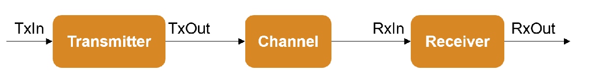
To aid in understanding the example, the following diagram illustrates the variable names for the waveforms that this example will create.
Modeling Approach and Methodology Overview
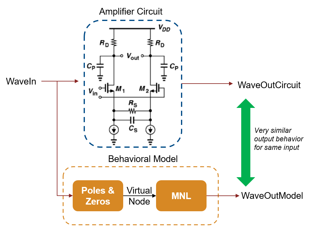
This example uses a linear pole/zero block followed by a memory-less nonlinearity block to model the peaking filter [2]. In the diagram below, the linear section of the model is labeled Poles and Zeros. To determine the parameters of this linear section, simulate the peaking filter circuit with a small signal waveform. This allows you to assume linearity, observe the output, estimate the linear transfer function and fit poles and zeros to it. Next, with a large signal swing stimulus, the output of the pole and zero block is compared to the output of the circuit. A function then maps the input voltage to the output voltage to form the memoryless nonlinearity (MNL) block model. The circuit and behavioral model block diagram are shown:
Model Validation Overview
The model validation will occur in two parts:
Validation with the modeling data,
Validation with new data.
Utilizing the data used to create the model, you can calculate the optimistic modeling error, which shows the expected error the model would be under the most favorable operating conditions. This step is a necessary one but not sufficient to prove a modeling success. The next stage of model checking utilizes a cross-validation approach, which uses different data patterns, amplitude swings and channel conditions to validate the accuracy of the model. The results of this validation will prove that the model structure and modeling approach are appropriate for the modeling task.
Simulation Setup
Setup a light weight SerDes simulation by defining the NRZ symbol time, data pattern, channel loss and transmit amplitudes. Ensure that the first transmit amplitude is in the small signal region of the peaking filter circuit so that it can be used to estimate the linear portion of the model. Also ensure that the last transmit amplitude is large enough to show the non-linear clipping of the peaking filter.
% Define System Parameters
symbolTime = 88e-12; %(seconds)
samplesPerSymbol = 16;

% Define additive circuit voltage noise (V)
noiseSigma = 0.00125;

% Define Channel loss (dB)
loss = 9;

% Define Data Pattern PRBS Order
PRBSOrder = 7;

% Define number of times to repeat pattern in total waveform to allow for
% any start up transients to settle out.
repeatPattern = 3;

% Define Tx peak amplitudes in Volts to explore.  The first and smallest
% amplitude will be used as the 'small signal' response.  The other
% amplitudes will be used to understand how larger voltages are impacted by
% the circuit nonlinearity.
txAmplitude = linspace(50,600,6)*1e-3;
Calculate the Data Pattern, Derived Constants and Plotting Collateral
Create the vector of data pattern voltages. Then derive the system parameters such as sample interval, number of samples, and number of amplitudes. Create the plotting time vector.
% Create vector of data pattern voltages.  Length is dependent on PRBS order only.
dataPattern = prbs(PRBSOrder,2^PRBSOrder-1)*2-1;

% Derived System Parameters
sampleInterval = symbolTime/samplesPerSymbol;
numberOfSamples = length(dataPattern)*repeatPattern*samplesPerSymbol;
numberOfAmplitudes = length(txAmplitude);

% Create plotting time vector, amplitude legend and shared zoom settings
t = sampleInterval*(0:numberOfSamples-1);
txAmplitudeLegend = cellstr(num2str(txAmplitude'*1000));
timeZoom = [1.15e-8 1.5e-8];
Initialize System Objects
Initialize the stimulus pattern generator, transmitter, channel and the peaking filter circuit. For the purposes of this example, the peaking circuit behavior is black box, where the only insight into it's behavior is through configuring the input and observing the output behavior. Feel free to look inside this System object™ to see how it is implemented.
% Initialize stimulus pattern generator
stimulus = serdes.Stimulus(...
    'SampleInterval',sampleInterval,...
    'SymbolTime',symbolTime,...
    'Specification','Symbol Voltage Pattern',...
    'Rj',0,...
    'DataPattern',dataPattern);

% Initialize transmitter block model
transmitter = serdes.VGA('Gain',1);

% Initialize channel model
channel = serdes.ChannelLoss(...
    'Loss',loss,...                       % Loss at target frequency (dB)
    'dt',sampleInterval,...               % Sample Interval
    'TargetFrequency', 1/symbolTime/2,... % Frequency for desired loss
    'TxR',50,'TxC',1e-14,...              % Near ideal Transmitter termination
    'RxR',50,'RxC',1e-14);                % Near ideal Receiver termination

% Initialize Rx circuit object.
rxCircuit = PeakingFilterCircuit('SampleInterval',sampleInterval,'SymbolTime',symbolTime);
Generate Waveforms
Create the transmitter input and output waveforms. Pass each transmitter output waveform through the same channel and through the peaking filter circuit.
% Create transmitter input waveform
txIn = zeros(numberOfSamples,1);
for ii = 1:numberOfSamples
    txIn(ii) = step(stimulus);
end

% Create transmitter Output waveform
txOut = zeros(numberOfSamples,numberOfAmplitudes);
for jj = 1:numberOfAmplitudes
    % Release transmitter system object to allow for setting of input property.
    release(transmitter)
    % Update amplitude
    transmitter.Gain = txAmplitude(jj);
    % Process waveforms
    txOut(:,jj) = transmitter(txIn);
end

% Pass each transmitter output waveform through the same channel.
rxIn = zeros(numberOfSamples,numberOfAmplitudes);
for jj = 1:numberOfAmplitudes
    % Release the channel system object to reset it and clear any memory.
    release(channel)
    % Pass transmitter waveform through channel.
    rxIn(:,jj) = channel(txOut(:,jj));
end

% Set the random number generator seed for randn to have the same results
% each time this example is run.
rng(1);

% Pass Rx input voltage waveforms through peaking filter Rx Circuit.  Noise
% is added to the circuit waveform for a more realistic waveform behavior.
rxOutCircuit = zeros(size(rxIn));
for jj = 1:numberOfAmplitudes
    release(rxCircuit) % Release circuit system object to clear out memory of prior processing.
    rxOutCircuit(:,jj) = rxCircuit(rxIn(:,jj)) + noiseSigma*randn(size(txIn));
end
Visualize Smallest Amplitude Response
View the smallest amplitude response for the input and output of the receiver and observe the small signal behavior.
plot(t,rxIn(:,1)*1e3,t,rxOutCircuit(:,1)*1e3)
grid on
xlabel('s')
ylabel('mV')
legend('RxIn','RxOut (circuit)')
title(sprintf('Receiver input/output waveforms for tx amplitude %g mV case',txAmplitude(1)*1e3))
axis([timeZoom -txAmplitude(1)*1e3 txAmplitude(1)*1e3])

Visualize Largest Amplitude Response
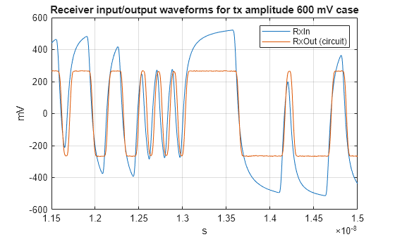
This plot of the receiver input and output for the largest transmit amplitude swing shows that the signal is severely clipped by the receiver as compared to the smallest amplitude case. This illustrates the non-linear nature of the receiver circuit and the challenge of creating a non-linear behavioral model that matches the circuit output characteristics.
plot(t,rxIn(:,end)*1e3,t,rxOutCircuit(:,end)*1e3)
grid on
xlabel('s')
ylabel('mV')
legend('RxIn','RxOut (circuit)')
title(sprintf('Receiver input/output waveforms for tx amplitude %g mV case',txAmplitude(end)*1e3))
axis([timeZoom -txAmplitude(end)*1e3 txAmplitude(end)*1e3])
Estimate Linear Transfer Function
The behavioral model is composed of two parts, the linear pole/zero block and the memory-less nonlinearity. To estimate the linear part of the model, analyze the system under conditions that do not excite the nonlinear behavior, by using the smallest amplitude transmit swing waveforms. With a presumed conditionally linear system, you can estimate the linear transfer function.
For a linear system characterized by its impulse response, , the output waveform, , is related to the input waveform, through convolution:
In the frequency domain, the convolution operation becomes multiplication:
With the frequency domain transfer function obtained through division:
While the math is very straightforward, the application of this process is made difficult by the realities of working with band-limited sampled data. For instance, the Discrete-Fourier Transform (DFT) of the sampled input waveform, , can contain excessive noise due to the Gibbs Phenomenon if care is not taken to minimize end-point discontinuities between the first and last sample, since the DFT assumes that the sampled waveform repeats itself. That is why we repeat the data pattern several times and choose a single repetition of the pattern of the overall waveform. Also choosing the second or a later repetition of the data pattern minimizes any start up transients. Further, the choice of the data pattern itself is important. While any random data pattern could be used, PRBS patterns have excellent spectral efficiency in that their frequency response envelope approaches the ideal power spectral density (PSD) of a sinc^2 response.
% Select a full repetition of the prbs data waveform.  More advanced
% analysis could average the PRBS data waveform like a benchtop sampling
% scope.

if repeatPattern < 3
    warning('Expected the data pattern to repeat at least 3 times.  Results may not be robust.');
end

% Determine the pattern length in samples
patLen = length(dataPattern)*samplesPerSymbol;

% Choose 2nd repetition of the waveform pattern.
secondPatternNdx = patLen+(1:patLen); % Second pattern index

% Get small signal input/output response from a single repetition of the
% data pattern.
inSmallSignal = rxIn(secondPatternNdx,1);
outSmallSignal = rxOutCircuit(secondPatternNdx,1);

% Extract the transfer function from the input and output frequency
% responses.
inFreqResponse = fft(inSmallSignal);
outFreqResponse = fft(outSmallSignal);
transferFunctionEstimate = outFreqResponse./inFreqResponse;

% Frequency vector for plotting
Fs = 1/sampleInterval; % Sampling Frequency
fk = (0:1:length(inSmallSignal)-1)'/length(inSmallSignal)*Fs; % Cyles/sample (Hz) vector
fkGHz = fk*1e-9;

% Upper limit of freqency domain plot at 2.2 times baud rate
fplotmax = 1/symbolTime*2.2*1e-9;

plot(fkGHz,db(inFreqResponse),fkGHz,db(outFreqResponse)), grid on
legend('Input','Output')
title('Frequency response')
xlabel('GHz')
ylabel('dB')
xlim([0 fplotmax])

The frequency responses have nulls at the baud rate, 1/symbolTime=11.3 GHz, showing that very little energy is transmitted at exactly this frequency. The upper limit of the fit is set to 3/4 of this fundamental frequency of the system as the amplified noise on the transfer function is ok up to this point.
% Upper fit limit.
freqFitLimit = 0.75/symbolTime;

plot(fkGHz,db(transferFunctionEstimate),freqFitLimit*[1 1]*1e-9,[-10 5],'--'), grid on
title('Estimated peaking filter transfer function')
xlabel('GHz')
ylabel('dB')
legend('Response','Fit limit')
axis([0 fplotmax -10 5])
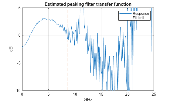
The estimated peaking filter transfer function is well behaved up until the first null of the frequency response where the division by very small numbers results in excessive numerical noise.
Fit Poles and Zeros to Estimated Linear Transfer Function
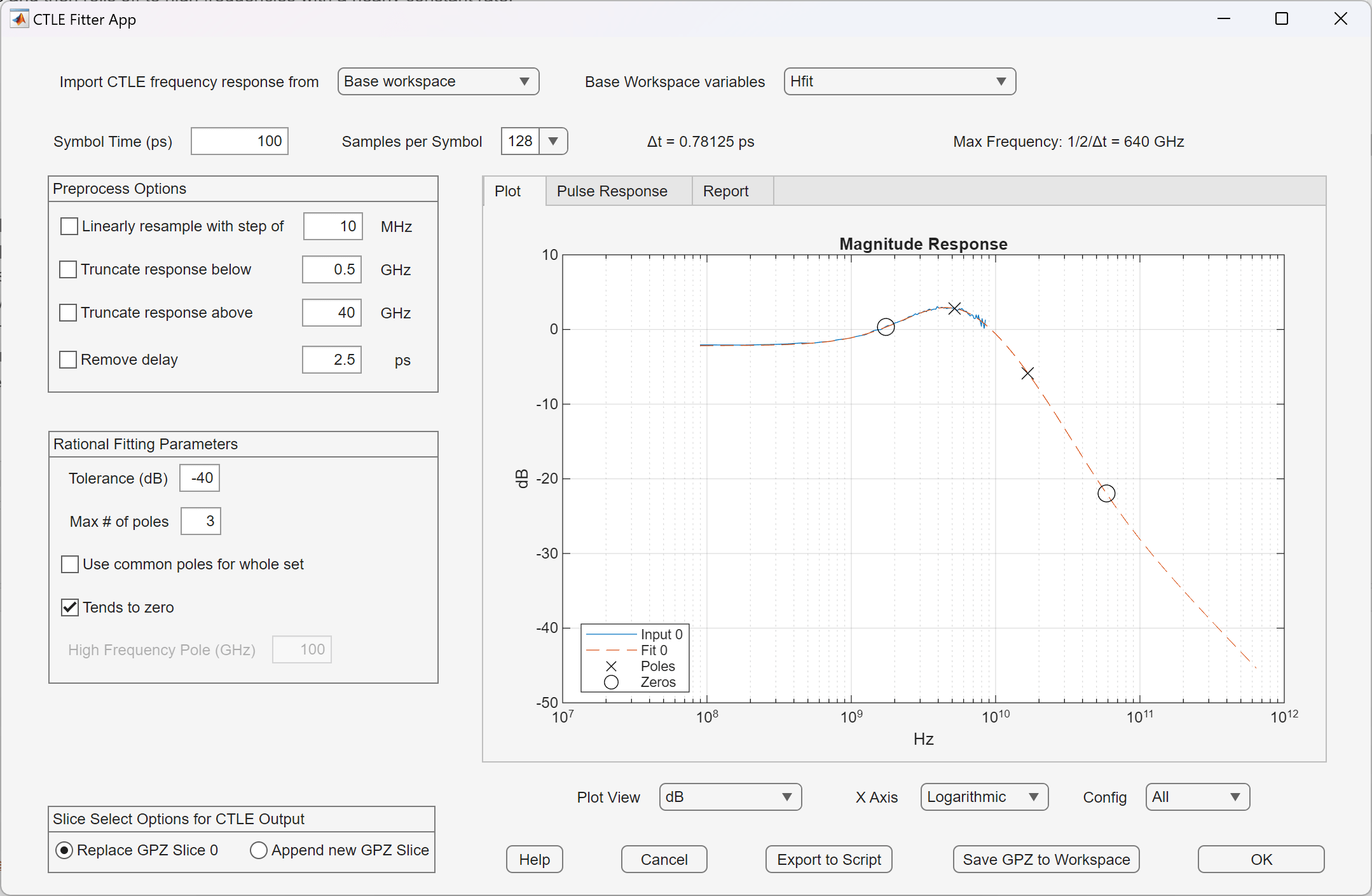
With the estimated (and noisy) peaking filter transfer function, use the rational fit methodology by using the CTLE Fitter app and ctlefit object. The fitting process does not provide any noise filtering, so it is important to pre-process the frequency response by truncating at a frequency below the first null in the response. When applying this methodology to modeling your own circuits, if you have access to an ac sweep simulation of the circuit, then a directly extracted peaking filter transfer function can replace the noise prone estimated peaking filter transfer function from time domain waveforms.
% Select the frequencies below the upper fit limit to avoid the first null
% at 1/SymbolTime.
freqSelect = fk<freqFitLimit;

% Create a column vector of frequency followed by tranfer functions for use
% in the CTLE fitter app.
Hfit = [fk(freqSelect),transferFunctionEstimate(freqSelect)];
The CTLE fitter app provides an interactive process to find the settings for a best fit. In this context, 'best fit' is one that captures the low frequency behavior, the peaking shape and then rolls off to high frequencies with a nearly constant rate.
% Launch CTLE fitter app
ctlefitter
From the top of the CTLE Fitter App, click the Base workspace variables parameter to select Hfit from the dropdown menu. This imports the base workspace variable into the app.
Experiment with the max number of poles with settings of
3, 5, 7and9maximum number of poles. From the report tab, note the fit error for each case.
Tradeoffs in Selecting the Number of Poles
You can represent a simple source degenerated differential amplifier without any parasitics by two poles and one zero [1]. This estimated peaking filter response of this example can be adequately represented by 3 poles. While the fit error does go down with more poles, the additional poles only fit the noise in the response and do not represent a better model. When the maximum number of poles is greater than 3, there are clusters of poles and zeros at nearly the same frequency which contribute little to the overall peaking filter shape and only complicate the model and could contribute to numerical instability if there are too many of them. An excellent practice when performing any kind of fitting is to use the simplest model that adequately characterizes the needed behavior. Due to the power spectral density of the input signal where the large majority of the signal energy is found at frequencies less than the baud rate, any fit errors at high frequencies are much less important than fit errors at low frequencies since the high frequency error is on the same order of magnitude as the numerical noise floor of the simulation. As long as the high frequency fit behavior is pretty close and rolls off at approximately 10 dB/decade, then we can be satisfied that the model is sufficient.
Using the setting determined in the app, update the next section of code with the
MaxNumberOfPolesandErrorToleranceused.
% Initialize ctleit object
fit = ctlefit(...
    'f',fk(freqSelect),...
    'H',transferFunctionEstimate(freqSelect),...
    'MaxNumberOfPoles',3,...
    'ErrorTolerance',-40,...
    'SampleInterval',7.8125e-13,...
    'TendsToZero',1,...
    'UseCommonPoles',0,...
    'PaddedPole',1e+11);

% Visualize fit magnitude with poles and zeros locations
plot(fit)

% Show fit report
report(fit)
19-Apr-2026 9:15:5.86753
CTLE with 1 Configurations
Fit response with a maximum of 3 poles
For ConfigSelect = 0
Fit error = -31.9263 dB
Gain: 0.785381 V/V or -2.0984 dB
Zeros:
100.924 GHz = | 100.924 + 0i |*1e9
-1.72924 GHz = | -1.72924 + 0i |*1e9
Poles:
-5.30861 GHz = | -4.53758 + 2.75529i |*1e9
-5.30861 GHz = | -4.53758 + -2.75529i |*1e9
-13.7351 GHz = | -13.7351 + 0i |*1e9
% Get gain/pole/zero (GPZ) matrix for use in the serdes.CTLE block.
gpz01 = fit.GPZ;
Create CTLE Model and Simulate the Virtual Node Waveform
You can process the receiver input waveform through the estimated poles and zeros to obtain a glimpse into what the receiver would look like if it were perfectly linear. This waveform is called the model virtual node. It is virtual since there is no place in the circuit where you can probe this behavior. This model virtual node behavior will be critical to modeling the last half of the receiver model, the memoryless non-linearity (MNL).
modelCTLE = serdes.CTLE(...
    'SymbolTime',symbolTime,...
    'SampleInterval',sampleInterval,...
    'WaveType','Sample',...
    'Mode',1,... % fixed mode
    'FilterMethod','Cascaded',...
    'Specification','GPZ Matrix',...
    'GPZ',gpz01);

% Create the virtual node waveform by passing the input Rx waveform through
% the pole/zero block for each tx amplitude.
modelVirtualNode = zeros(size(rxIn));
for jj = 1:numberOfAmplitudes
    release(modelCTLE)
    modelVirtualNode(:,jj) = modelCTLE(rxIn(:,jj));
end

% Visualize smallest and largest amplitude waveforms of the virtual node.
plot(t,modelVirtualNode(:,[1,numberOfAmplitudes])*1e3),
grid on,
title('Model interior virtual node')
leg2a = legend(txAmplitudeLegend([1,numberOfAmplitudes]));
leg2a.Title.String = 'Tx amplitude (mV)';
xlabel('s'),ylabel('mV')
axis([timeZoom -txAmplitude(end)*1e3 txAmplitude(end)*1e3])
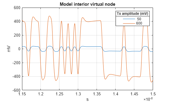
Note that this response is linear. If you multiply the 50 mV amplitude waveform by 12, you will exactly get the 600 mV amplitude waveform.
Memory-Less Nonlinearity (MNL)
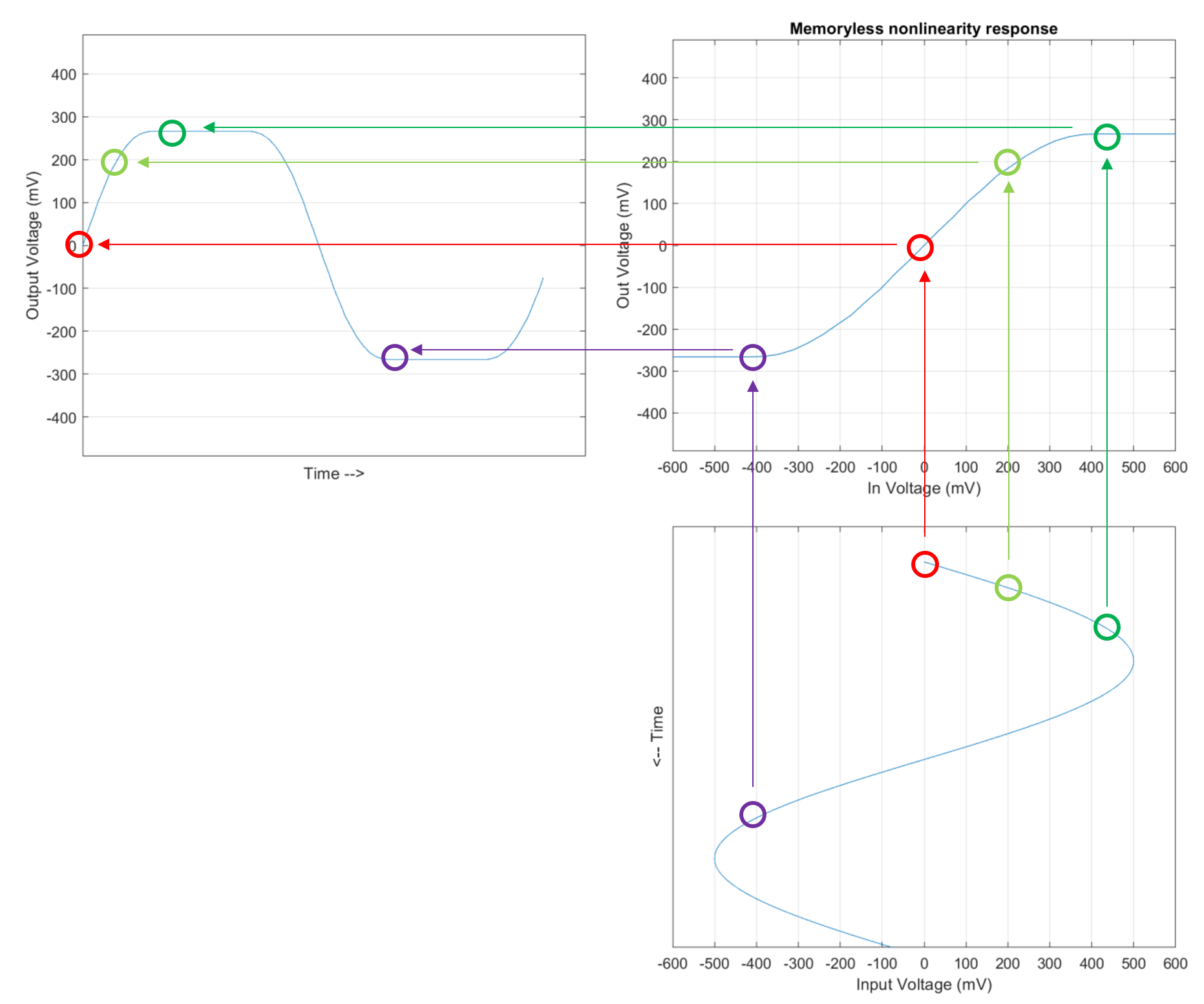
A memory-less nonlinearity is a function where the output at time t is only dependent on the input at the same time t. This means that the function has no memory of prior inputs and is thus "memory-less". The following graphic shows how input voltages are mapped to the output voltage using the MNL response. It is essential that this response is a function where each input value is uniquely mapped to an output value. The implementation of such a MNL in the System object, serdes.SaturatingAmplifier, is through a lookup table with linear interpolation between data points.
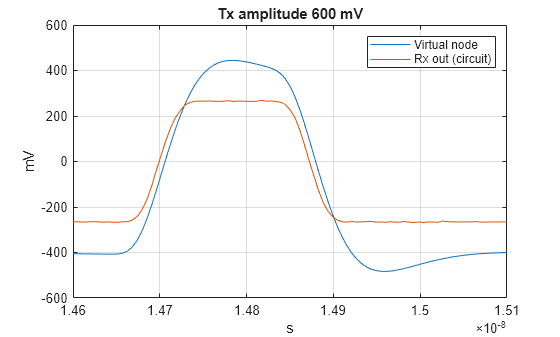
Next, we inspect the time domain waveforms at the input to the MNL (the virtual node) and the output of the MNL (the circuit receiver out) waveforms for the largest transmit amplitude.
plot(t(secondPatternNdx),modelVirtualNode(secondPatternNdx,end)*1e3,t(secondPatternNdx),rxOutCircuit(secondPatternNdx,end)*1e3)
legend('Virtual node','Rx out (circuit)'),
grid on
title(sprintf('Tx amplitude %g mV',txAmplitude(end)*1e3))
xlabel('s')
ylabel('mV')
timeZoomForAlign = [1.46e-8 1.51e-8];
axis([timeZoomForAlign -txAmplitude(end)*1e3 txAmplitude(end)*1e3])
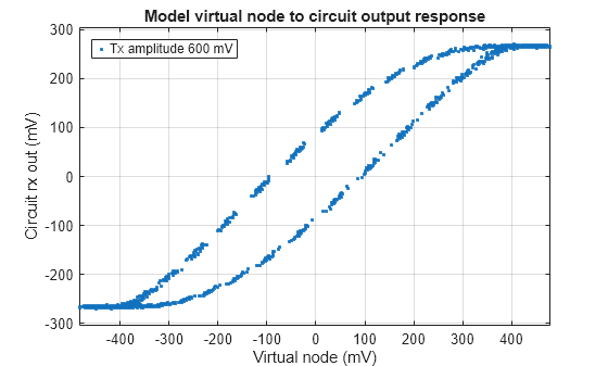
Plotting the virtual node versus the receiver circuit output does not show a functional relationship where a single input voltage is mapped to a single output voltage as is needed for a MNL. If there are loops or multiple signal trajectories in the below plot, then it means that the input/output relationship still has some degree of memory that needs to be compensated for, either with a better pole/zero model or in the case of this example, the removal of a simple delay. This delay is due to the serdes.CTLE block adding a single extra sample of delay to the output waveform. This sort of delay is inconsequential for the model but needs to be compensated for before estimating the MNL.
plot(modelVirtualNode(secondPatternNdx,end)*1e3,rxOutCircuit(secondPatternNdx,end)*1e3,'.')
grid on
xlabel('Virtual node (mV)'),
ylabel('Circuit rx out (mV)')
legend(sprintf('Tx amplitude %g mV',txAmplitude(end)*1e3),'Location','NorthWest')
title('Model virtual node to circuit output response')
axis equal
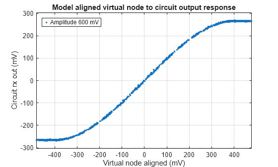
By aligning the two waveforms, we see that there is a straightforward 1:1 mapping relationship between the two which can be modeled with a MNL.
% Align virtual node with circuit output
modelVirtualNodeAligned = AlignWaveforms(rxOutCircuit,modelVirtualNode);

plot(t(secondPatternNdx),modelVirtualNodeAligned(secondPatternNdx,end)*1e3,t(secondPatternNdx),rxOutCircuit(secondPatternNdx,end)*1e3)
legend('Aligned virtual node','Rx out (circuit)'),
grid on
title(sprintf('Tx amplitude %g mV',txAmplitude(end)*1e3))
xlabel('s')
ylabel('mV')
axis([timeZoomForAlign -txAmplitude(end)*1e3 txAmplitude(end)*1e3])

plot(modelVirtualNodeAligned(secondPatternNdx,end)*1e3,rxOutCircuit(secondPatternNdx,end)*1e3,'.')
grid on
xlabel('Virtual node aligned (mV)'),ylabel('Circuit rx out (mV)')
legend(sprintf('Amplitude %g mV',txAmplitude(end)*1e3),'location','NorthWest')
title('Model aligned virtual node to circuit output response')
axis equal
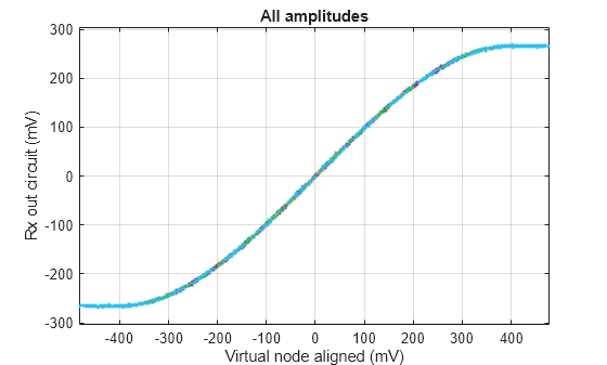
Next, look at all the waveforms from all the amplitudes to ensure that the functional relationship is consistent for sets of input versus output behavior.
% Get virtual node waveforms and rx circuit out waveforms for all amplitudes
tmpVirtualNode = modelVirtualNodeAligned(secondPatternNdx,:);
tmpVRxOutCircuit = rxOutCircuit(secondPatternNdx,:);

plot(tmpVirtualNode*1e3,tmpVRxOutCircuit*1e3,'.','MarkerSize',4)
grid on
xlabel('Virtual node aligned (mV)'),ylabel('Rx out circuit (mV)')
title('All amplitudes')
axis equal
Modeling Memoryless Nonlinearity
With all this input/output data, we need to fit some type of model to it. The MNL itself will be implemented with the serdes.SaturatingAmplifier block which requires a tabulated voltage in versus voltage out response. There are two different modeling methodologies to choose from: parametric estimation and non-parametric estimation. The parametric estimation approach would be to fit some type of hyperbolic tangent or a generalized logistic function to the data. Then the function could be sampled to provide the needed input for the serdes.SaturatingAmplifier implementation. A non-parametric estimation approach would represent the relationship as several discrete points and directly estimate tabulated voltage in / voltage out response.
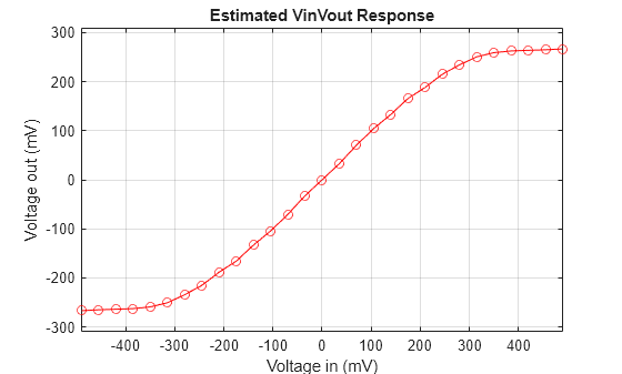
For simplicity, this example uses a non-parametric estimation approach here, which is bin and average, as illustrated below. First the data is horizontally separated into several bins. Then within each bin, the vertical axis values (the circuit output voltage) are averaged to reconcile any variation. The center of the bin and average form the tabulated voltage in versus voltage out response. This approach will yield sufficient results if an adequate number of bins are used such that the piece-wise linear result has minimal deviation from the data. In the illustration, only 7 bins are used, and it can be observed that the second and the second to last bin average have a slight bias to them, which could have been reduced if more bins were utilized. For this example, we use 29 horizontal bins so it shouldn't have this issue.
The downside of the empirical bin and average approach is that there is no guarantee that the result is symmetric and monotonic as required by the serdes.SaturatingAmplifier block. Therefore, an additional step of forcing symmetry and monotonicity is taken. The symmetry assumption is good for differential signals and ensures that the voltage in / voltage out response is balanced. The monotonic condition is required to ensure that there is no ambiguity in the 1:1 voltage mapping of the response.
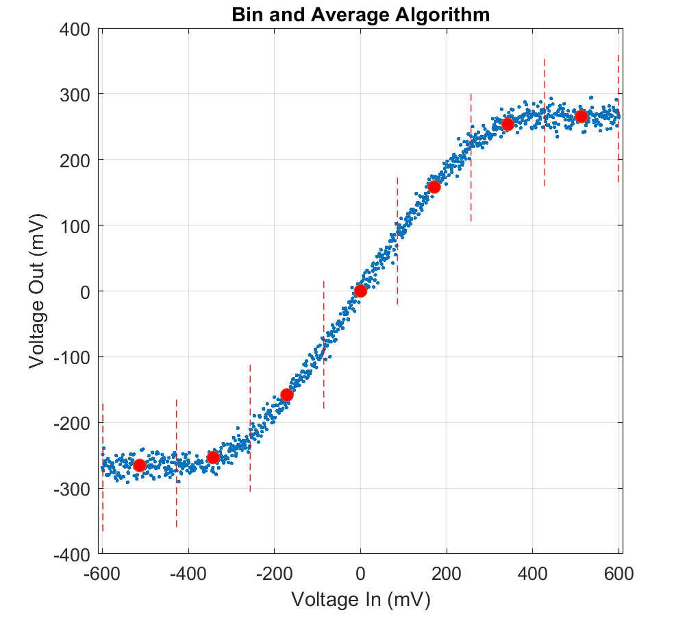
% Determine maximum input voltage
maxVin = max(abs(tmpVirtualNode(:)));

% Bin edges vector must be symmetric and even in length to guarantee 0 is a bin center.
vinBinEdges = linspace(-maxVin*(1+1/20),maxVin*(1+1/20),30);

% Bin centers is the average of the bin edges
vinBinCenters = (vinBinEdges(1:end-1) + vinBinEdges(2:end))/2;

% For each bin, find the voltage input data sample locations between the lower
% and upper edges. Find the voltage output data at these locations and find
% their average value to determine the output voltage response.
voutBinAverage = zeros(size(vinBinCenters));
for ii = 1:length(vinBinEdges)-1
    ndx = tmpVirtualNode(:) > vinBinEdges(ii) & tmpVirtualNode(:) <= vinBinEdges(ii+1);
    voutBinAverage(ii) = mean(tmpVRxOutCircuit(ndx));
end

% Enforce symmetry and monotonicity to smooth response
voutBinAverage = enforceMonotonicMNL(voutBinAverage);

plot(vinBinCenters*1e3,voutBinAverage*1e3,'-or')
grid on, axis equal
xlabel('Voltage in (mV)'),ylabel('Voltage out (mV)')
title('Estimated VinVout Response')
Create Memoryless Nonlinearity Model Block
Create the saturating amplifier block and process the model virtual node waveform to obtain the model output.
% Create VinVout matrix for SaturatingAmplifier block
vinVout = [vinBinCenters(:),voutBinAverage(:)];

% Memoryless nonlinearity block
modelMNL = serdes.SaturatingAmplifier(...
    'Specification','VinVout',...
    'VinVout',vinVout);

% Apply memoryless nonlinearity to model virtual node (unshifted)
rxOutModel = zeros(size(modelVirtualNode));
for jj = 1:numberOfAmplitudes
    rxOutModel(:,jj) = modelMNL(modelVirtualNode(:,jj));
end
Modeling Data Validation
Validation gives you the confidence we need to use the model to predict future behavior. The first validation task is to compare the behavioral model's output to the circuit output over the same data set that was used to create the model. This is a necessary step but is not sufficient to prove that you have a good model. That proof will come later in the cross-validation step. Since this data was used to create the model, it is expected to show the minimum error possible with the model. The model error due to other data patterns and amplitudes will not be likely to be less than the model error seen here.
% Align model waveform with circuit waveform
[rxOutModelAligned,modelIsValidFlag]=AlignWaveforms(rxOutCircuit,rxOutModel);

% Error between circuit and model
errorRxOut = rxOutCircuit-rxOutModelAligned;

% Calculate RMS and max absolute error
errorRMS = rms(errorRxOut(modelIsValidFlag,:),1);
errorMax = max(abs(errorRxOut(modelIsValidFlag,:)),[],1);

% Determine index of max error for automatic plot zoom
[~,maxAmp1Ndx]=max(abs(errorRxOut(:,1)));
[~,maxAmp5Ndx]=max(abs(errorRxOut(:,6)));
Compare Circuit Versus Model Behavior at Lowest Amplitude
Comparing the circuit and model output waveform for the lowest amplitude signal, shows a good correlation with the largest error due to the additive random noise. It would be interesting to see the impact on the modeling error a reduction in the additive random noise due to averaging together multiple repetitions of the data pattern. The error response also displays a small 2 mV systematic offset correlated with the data pattern itself, perhaps a slight manual adjustment to the DC gain of the poles and zeros block could reduce this error further.
% Visualize
figure
validateAxisA(1) = subplot(211);
plot(t,rxOutCircuit(:,1)*1e3,t,rxOutModelAligned(:,1)*1e3)
legend('Circuit','Model')
title(sprintf('RxOut waveform comparison at tx amplitude of %g mV',txAmplitude(1)*1000))
ylabel('mV')
xlabel('s')
grid on

validateAxisA(2) = subplot(212);
plot(t,errorRxOut(:,1)*1e3)
ylabel('mV'),xlabel('s')
grid on
legend('Error = circuit - model')
linkaxes(validateAxisA,'x')
xlim([t(maxAmp1Ndx)-10*symbolTime,t(maxAmp1Ndx)+10*symbolTime])

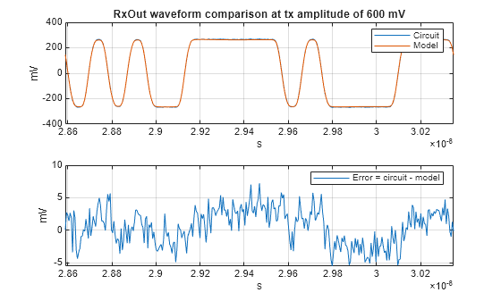
Compare Circuit Versus Model Behavior at Largest Amplitude
Comparing the circuit and model output waveform for the largest amplitude signal, shows excellent correlation. The error does have a slight correlation with the data pattern but the signal strength (about 260 mV) to maximum error (about 7 mV) ratio is greater than 30 dB which is quite good.
figure
validateAxisB(1) = subplot(211);
plot(t,rxOutCircuit(:,numberOfAmplitudes)*1e3,t,rxOutModelAligned(:,numberOfAmplitudes)*1e3)
legend('Circuit','Model')
title(sprintf('RxOut waveform comparison at tx amplitude of %g mV',txAmplitude(numberOfAmplitudes)*1000))
ylabel('mV'),xlabel('s')
grid on

validateAxisB(2) = subplot(212);
plot(t,errorRxOut(:,numberOfAmplitudes)*1e3)
ylabel('mV'),xlabel('s')
legend('Error = circuit - model')
grid on

linkaxes(validateAxisB,'x')
xlim([t(maxAmp5Ndx)-10*symbolTime,t(maxAmp5Ndx)+10*symbolTime])
Summarize Model Error
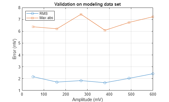
The figure below shows the maximum absolute error and root-mean-square (RMS) error for all of the amplitudes of the modeling data set. While the maximum error for each case is usually due to differences at symbol transition regions, the RMS error gives a more overall measure of the difference of the model and circuit behavior. A few mV of RMS error is evidence of a very good model to circuit correlation.
figure
plot(txAmplitude*1000,errorRMS*1e3,'-o',txAmplitude*1000,errorMax*1e3,'-s'), grid on
xlabel('Amplitude (mV)'),ylabel('Error (mV)'), title('Validation on modeling data set')
legend('RMS','Max abs','Location','northwest')
Cross-Validation Introduction
As mentioned previously, the cross-validation is essential in proving that the model can accurately predict behavior outside of the parameter space that was used to create it. A model that can survive robust cross-validation is an asset to understanding the system and performing follow on surrogate analysis. For this cross validation, we will utilize a different random data pattern, a different amount of channel loss and different transmit amplitudes.
Setup Cross-Validation
Here we use different the transmit amplitudes, data pattern and channel loss from the ones used in the modeling data set to show that the model is invariant to these types of factors.
% Define new Tx amplitudes
txAmplitudeXV = linspace(40,700,5)*1e-3;

% Define new NRZ data pattern.
dataPatternXV = (randi(2,1,100)-1)*2-1;

% Change channel loss
release(channel)
channel.Loss = 5;

% Number of amplitudes for cross-validation
nAmplitudeXV = length(txAmplitudeXV);

% Stimulus
numberOfSamplesXV = length(dataPatternXV)*repeatPattern*samplesPerSymbol;
stimulusXV = serdes.Stimulus(...
    'SampleInterval',sampleInterval,...
    'SymbolTime',symbolTime,...
    'Specification','Symbol Voltage Pattern',...
    'DataPattern',dataPatternXV);
Generate New Input Waveform and Circuit Output Waveform for Cross-Validation
The cross-validation stimulus is first created and then scaled by the desired amplitude before passing it through the channel and receiver blocks.
% Transmitter Input waveform
txInXV = zeros(numberOfSamplesXV,1);
for ii = 1:numberOfSamplesXV
    txInXV(ii) = step(stimulusXV);
end

% Set random number generator seed
rng(2);

% Create new receiver circuit output waveform
rxInXV = zeros(numberOfSamplesXV,nAmplitudeXV);
rxOutCircuitXV = zeros(size(rxInXV));
for jj = 1:nAmplitudeXV
    % Release and reset blocks with memory
    release(transmitter)
    release(channel)
    release(rxCircuit)

    % Update transmitter swing
    transmitter.Gain = txAmplitudeXV(jj);

    % Determine Rx In and Rx Out waveform
    rxInXV(:,jj) = channel(transmitter(txInXV));
    rxOutCircuitXV(:,jj) = rxCircuit(rxInXV(:,jj)) + noiseSigma*randn(size(txInXV));
end
Generate Model Output Waveform
Provided the cross-validation waveform at the input of receiver, pass the waveform through the model CTLE and model MNL blocks.
% Given the Rx In waveform, apply CTLE model block and memoryless nonlinearity model block to
% obtain the model output waveform.
rxOutModelXV = zeros(size(rxInXV));
for jj = 1:nAmplitudeXV
    release(modelCTLE)
    rxOutModelXV(:,jj) = modelMNL(modelCTLE(rxInXV(:,jj)));
end
Compare Circuit Waveforms to Model Waveforms
Align model and circuit waveforms for accurate error waveform calculations.
% Align model waveform with circuit waveform
[rxOutModelXVAligned,isValidFlagXV]=AlignWaveforms(rxOutCircuitXV,rxOutModelXV);

% Time vector for validation
tXV = sampleInterval*(0:numberOfSamplesXV-1);

% Difference between circuit behavior and model
errorRxOutXV = rxOutCircuitXV-rxOutModelXVAligned;

% Error metrics
errorRMSXV = rms(errorRxOutXV(isValidFlagXV,:),1);
errorMaxXV = max(abs(errorRxOutXV(isValidFlagXV,:)),[],1);

% Determine index of max error for automatic plot zoom
[~,maxAmp1Ndx]=max(abs(errorRxOutXV(:,1)));
[~,maxAmp5Ndx]=max(abs(errorRxOutXV(:,5)));
Compare Circuit Versus Model Behavior at Smallest Amplitude
For the smallest amplitude cross-validation waveform, the circuit to model correlation is dominated by additive random noise and has a similar error magnitude to the modeling data set. The error does appear completely random and displays a correlation with the data pattern itself but. As suggested earlier, this may be possible to reduce with a manual adjustment of the pole and zero block DC gain.
% Visualize
figure
validateAxisC(1) = subplot(211);
plot(tXV,rxOutCircuitXV(:,1)*1e3,tXV,rxOutModelXVAligned(:,1)*1e3)
legend('Circuit','Model')
title(sprintf('RxOut waveform cross-validation comparison at tx amplitude of %g mV',txAmplitudeXV(1)*1000))
ylabel('mV'),xlabel('s')
grid on

validateAxisC(2) = subplot(212);
plot(tXV,errorRxOutXV(:,1)*1e3)
ylabel('mV'),xlabel('s')
grid on
legend('Error = circuit - model')

linkaxes(validateAxisC,'x')
xlim([t(maxAmp1Ndx)-10*symbolTime,t(maxAmp1Ndx)+10*symbolTime])
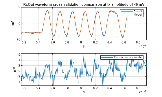
Compare Circuit Versus Model behavior at Largest Amplitude
For the largest amplitude cross-validation waveform, the circuit to model correlation is excellent. The maximum error, about -10.2 mV, occurs at the edge of a symbol transition and illustrates the difficulty of perfecting aligning band-limited sampled data. This type of difference is more an artifact of the error calculation itself than an indication of a modeling deficiency. In practical systems with jitter, this type of difference is mostly unavoidable.
figure
validateAxisD(1) = subplot(211);
plot(tXV,rxOutCircuitXV(:,nAmplitudeXV)*1e3,tXV,rxOutModelXVAligned(:,nAmplitudeXV)*1e3)
legend('Circuit','Model')
title(sprintf('RxOut waveform cross-validation comparison at tx amplitude of %g mV',txAmplitudeXV(nAmplitudeXV)*1000))
ylabel('mV'),xlabel('s')
grid on

validateAxisD(2) = subplot(212);
plot(tXV,errorRxOutXV(:,nAmplitudeXV)*1e3)
ylabel('mV'),xlabel('s')
legend('Error = circuit - model')
grid on

linkaxes(validateAxisD,'x')
xlim([t(maxAmp5Ndx)-10*symbolTime,t(maxAmp5Ndx)+10*symbolTime])

Summarize Model Error
Comparing the cross-validation error summary with the modeling data set error summary, it is interesting to note that the RMS error is roughly flat as the waveform amplitude increases for both data sets, but the RMS error increases with amplitude for the cross-validation data set as compared with the model data set. This is likely due to differences at the symbol transition regions of the waveform where a small amount of misalignment can result in large voltage differences. This illustrates the robustness of the RMS error metric in comparing performance of data sets.
Note how the RMS and maximum error is greater for the cross-validation than for the modeling data validation. It is always critical to fully stress-test a model that will be used outside of the data set used to create it and ensure that any error is acceptable to the application.
figure
plot(txAmplitudeXV*1000,errorRMSXV*1e3,'-o',...
    txAmplitudeXV*1000,errorMaxXV*1e3,'-s'), grid on
xlabel('Amplitude (mV)'),
ylabel('Error (mV)'),
title('Cross validation')
legend('RMS','Max abs','location','northwest')

What should you do when the validation results are poor? Here are some recommendations:
Reduce or eliminate sources of uncertainty in the modeling and validation data. In a lab setting, average the waveforms to minimize random error. In a circuit simulation setting, turn off any noise and jitter settings.
Is the estimated frequency transfer function noisy? Ensure that any endpoint discontinuities are minimized and that a PRBS pattern is used for the linear portion of the model.
Perhaps modify the assumed model of the peaking filter. We have a used a pole/zero block followed by an MNL. Other model structures are possible like pole/zero + MNL + pole/zero, or MNL + pole/zero + MNL [2]. Each non-linear system is unique in its own way and the better you can understand and emulate the structure of the system with the model the better.
Does the observed voltage in versus voltage out response have loops or distinct trajectories? This is an indication that there is still memory that needs to be separated out before the MNL can be estimated.
Conclusion
This example shows how to model a non-linear CTLE or peaking filter circuit when only the input and output behavior of the circuit is available, this type of process is often called black-box modeling [3]. When more information about the system is known, it is no longer a black box but perhaps a gray box and it is important to modify the modeling approach to encompass this additional knowledge. This hybrid approach is often necessary for non-linear modeling as each non-linear system is unique in some unknown way.
One of the advantages of the source degenerated differential amplifier circuit is the ability to change the peaking gain and peaking frequency by modifying the source resistor and capacitor. Therefore, most peaking filters have a number of configurations which the user can choose from to provide more or less equalization based on the channel loss. This example illustrates how a single configuration can be modeled and can be applied to model a whole family of CTLE or peaking filter configurations with a few modifications.
Lastly, actual circuit behavior will be different from the idealized peaking filter circuit System object. Feel free to look under the hood at the white-box code of the PeakingFilterCircuit to see how well the modeling approach was able to recreate the parameters of this block.
Further Exploration
Experiment with the modeling data pattern. What happens if you use a random data pattern like
dataPattern = (randi(2,1,100)-1)*2-1instead of a PRBS pattern?Experiment with the PRBS order. The example uses a PRBS7 which is 127 bits long. What is the impact of using a higher or lower order PRBS on the estimated linear transfer function?
How does the accuracy of the modeling results change when the channel loss is varied?
How does the system symbol time impact the modeling results? How does the signal power spectral density change with symbol time?
How does the additive circuit voltage noise impact the modeling results?
How does
freqFitLimit = 0.75/symbolTime, impact the modeling results?What impact would random jitter have on the modeling process? Modify the stimulus System object call by setting the Rj jitter parameter to
0.02UI.Experiment with modifying the
PeakingFilterCircuitto have additional stages of poles/zeros and memoryless nonlinearities. How does that impact the modeling methodology?
References
[1] Palermo, S. (2024, September 10). ECEN720: High-Speed Links, Circuits and Systems Spring 2014, Lecture 8: RX FIR, CTLE & DFE Equalization [PowerPoint slides]. https://people.engr.tamu.edu/spalermo/ecen689/lecture8_ee720_rxeq.pdf
[2] https://en.wikipedia.org/wiki/Nonlinear_system_identification