Implement Crossbar (X-BARs) Functionality with C2000 Microcontroller Blockset
This example shows how to use the Input, Output and ePWM X-BARs available on some of the TI® processors using C2000™ Microcontroller Blockset.
In this example, you will learn how to implement the following workflows on TI F28379D LaunchPad.
Route the signal at the GPIOs configured as output pins to peripherals through the Input X-BAR.
Configure multiple signals through different MUXes available in the ePWM X-BAR to provide the TRIP inputs to the ePWM modules.
Configure the digital compare (DC) module in the ePWM block to process the TRIP inputs and generate trip events to the Trip Zone (TZ) module in the ePWM block.
Configure the Trip Zone (TZ) module to generate an EPWMx_TZINT to CPU PIE.
Configure multiple signals through different MUXes available in the Output X-BAR to drive the output GPIO pins.
Prerequisites
Complete the following tutorials:
Required hardware
TI F28379D LaunchPad. For your convenience, a preconfigured f2837xXBAR model is used in this example.
Hardware Connections
Perform the following hardware board connection externally.
The positive input for CMPSS1H is the output of DAC-A and the positive input for CMPSS2L is the output of DAC-B.

To monitor the signal from the output X-BARs in the scope and the data inspector, route the signals to the GPIO pins and read in the model.
The signal from Output X-BAR1 is externally connected to GPIO16 and the signal from Output X-BAR2 is externally connected to GPIO27.

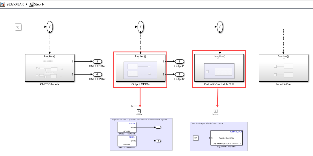
Model
Open the f2837xXBAR.slx model.

The GPIO11 and GPIO14 are configured as digital output. You can toggle these GPIO pins using the toggle switch in the model.
The signals at GPIO11 and GPIO14 pins are routed via the Input X-BARs to the ePWM X-BARs and Output X-BARs.
CMPSS1H and CMPSS2L positive inputs are driven from DAC A and DAC B output respectively.
The CMPSS1 TRIPH signal and Input X-BAR2 signals are combined using an OR logic operation and sent to ePWM TRIP 4 via ePWM X-BAR. Similarly, the CMPSS2 TRIPL signal and Input X-BAR1 signals are combined using an OR logic operation and sent to ePWM TRIP 5.
The ePWM TRIP4 and TRIP5 are configured as ePWM Digital Compare events DCAEVT2 and DCBEVT2 to trip ePWM output.
The CMPSS TRIP signal and Input X-BAR signals are combined using an OR logic operation and sent to GPIO using Output X-BAR.
Crossbar (X-BAR) Signal Routing
The figure shows the routing of multiple signals through the X-BAR.

Configure and Run the model
1. Open the f2837xXBAR.slx model. This model is configured for TI F28379D LaunchPad hardware. To run the model on other TI C2000 processors, press Ctrl+E to open the Configuration Parameters dialog box and follow the below steps.
2. In the Configuration Parameters window, click Hardware Implementation.
3. Browse to Target Hardware Resources > Input X-BAR. Configure Input1 pin assignment and Input2 pin assignment to read data from GPIO14 and GPIO11 respectively.

4. Browse to Target Hardware Resources > Output X-BAR. CMPSS1 TRIPOUTH signal from MUX 0 and Input X-BAR2 signal (GPIO 11) from MUX 3 is ORed and sent to Output1. Output X-BAR1 signal is routed to GPIO24. Similarly, CMPSS2 TRIPOUTL signal from MUX 3 and Input X-BAR1 signal (GPIO 14) from MUX1 is ORed and sent to GPIO25 via Output X-BAR2

5. To monitor the output signals from output X-BAR, output1 signal from GPIO24 is externally connected to GPIO16. Similarly, output2 signal from GPIO25 is externally connected to GPIO 27. Both the GPIO16 and GPIO27 are configured as input pins in the model. To run the model in external mode, select Enable OUTPUT# latch from output X-BAR.
6. Browse to Target Hardware Resources > ePWM. CMPSS1 TRIPH signal from MUX 0 and Input X-BAR2 signal (at GPIO 11) from MUX 3 is ORed and is passed as ePWM TRIP4 signal. Similarly, CMPSS2 TRIPL signal from MUX 3 and Input X-BAR1 signal(at GPIO 27) from MUX1 is ORed and is passed as ePWM TRIP5 signal.

6. Click Apply and OK.
7. The Output X-BAR latch is cleared using Register Read/Write block after the data is read by the Digital Input blocks. To ensure the sequence is followed, the Function Split block is used to execute the clearing of latch after the data has been read from the Digital Input blocks.
8. In the ePWM block, TRIP4 and TRIP5 are used as source for DCAEVT2 and DCBEVT2, respectively.

9. The DCAEVT2 and DCBEVT2 are configured as CBC Trip events. ePWMxA is Forced to move lower in priority in case of a trip. The interrupts for these events are also enabled.

10. The ePWM TZ ISR for DCAEVT2 and DCBEVT2 is triggered using the Hardware interrupt block.

11. Click the Hardware mapping on the block to view the interrupt configurations.

12 In EPWM1_TZ_DCAEVT2 Interrupt subsystem, DACHVALS of CMPSS1 is set to 4095 and GPIO11 is set to low to clear the trip conditions for ePWM1. This is done to reevaluate the trip conditions every cycle.
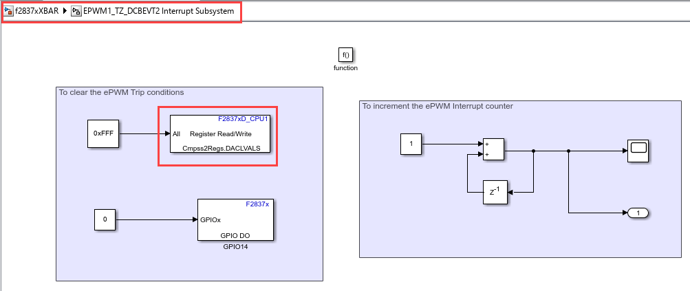
Similarly, in EPWM1_TZ_DCBEVT2 Interrupt subsystem, DACLVALS of CMPSS2 is set to 4095 and GPIO14 is set to low.
13. Configure the CMPSS and DAC configuration as mentioned in the Using Comparator Subsystem (CMPSS) for Voltage Compare example.
14. Open Hardware tab and click Monitor & Tune. You can view the signals on the Scope block and Simulink Data Inspector.
Analysis of DAC, CMPSS and Output X-BAR signals
DAC input, CMPSS status output and Output XBAR signal are sent to the scope.
Output XBAR signal is logical OR of Input XBAR signal and CMPSS TRIP signal.
The ePWM TRIP input is also the logical OR of Input XBAR signal and CMPSS TRIP signal. The Output X-BAR signal represents the state of ePWM TRIP signals.
If either of the signals are high, the output XBAR signal is also high.
DAC A is positive input to CMPSS1 and DAC B is positive input to CMPSS2. The input to DAC are manual switches.
When positive input is greater than the negative input, the CMPSS TRIP out is high.
Input X-BAR is mapped to GPIO11 and GPIO14. These are toggle switches.
The following table describes the expected results.

The image here displays the waveform for condition 4 from the table.

The image here displays the waveform for condition 5 from the table.
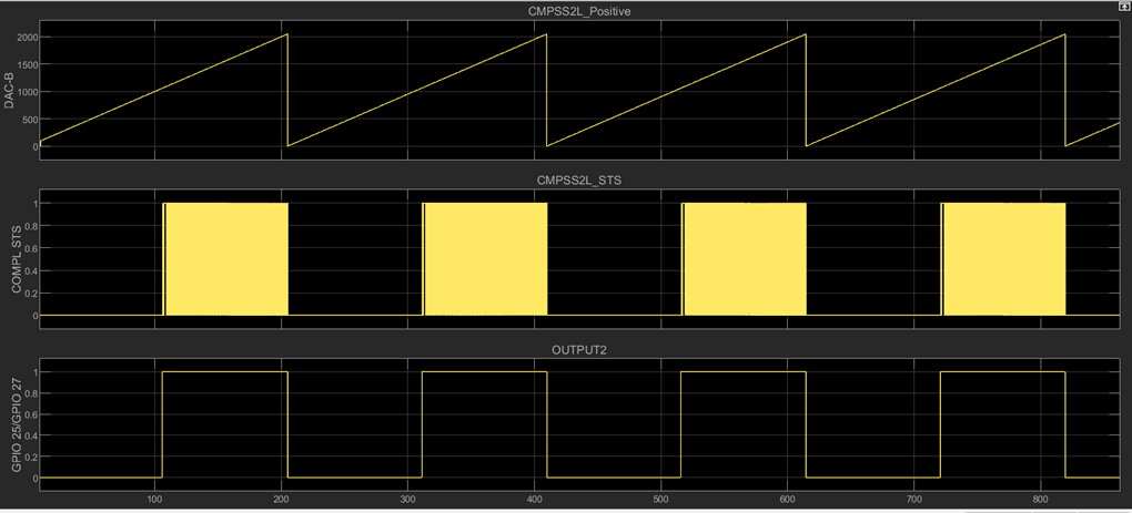
Note: The signals COMPH STS and COMPL STS in the above plots are toggled as the Cmpss1Regs.DACHVALS and Cmpss2Regs.DACLVALS values are reset to 0xFFF in EPWM1_TZ_DCAEVT2 and EPWM1_TZ_DCBEVT2 subsystems.
Other things to try:
Try different combinations of MUX signals in ePWM and Output X-BAR.
Try ePWM One Shot Trip.