Implement Signal Routing Using C2000 Crossbar (X-BAR)
The C2000™ crossbar (X-BAR) provides flexibility to connect device inputs, outputs, and internal resources in a wide range of configurations. There are different X-BARs depending on the signal routing. Each X-BAR is named according to where it routes the signals.
For example:
The Input X-BAR and CLB Input X-BAR route external signals In to the device.
The Output X-BAR and CLB Output X-BAR route internal signals Out of the device to a GPIO.
The CLB X-BAR and ePWM X-BAR route signals to the CLB and ePWM modules, respectively
The configuration of Input, Output, CLB (Configurable Logic Block) and ePWM X-BARs are configured in Simulink® model configuration parameters.
Input X-BAR
The Input X-BAR routes signal from a General Purpose Input/Output to different peripherals such as ADC, eCAP, ePWM, and external interrupts. The input of each Input X-BAR instance (INPUTx) can be any GPIO, while the output of each instance connects to a specific peripheral on the device. The following diagram illustrates how the Input X-BAR interfaces with the F2838x family of processors.

Note
The output connection of each Input X-BAR might vary depending on the processor family.
Configure Input X-BAR
You can configure the GPIO input to each Input X-BAR instance in the Simulink model under Hardware Implementation > Target hardware resources > Input X-BAR.
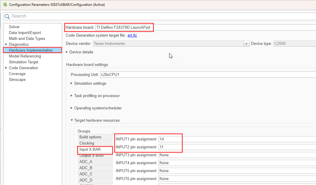
You can add any valid GPIO number for the given target hardware.
Note
You can route the GPIOs that you configure as digital outputs to the device using Input X-BAR.
The output of each instance connects to a specific peripheral. You can view the connections in the configuration parameters of the peripheral. For example, You can view the Input X-BAR corresponding to the ePWM under Hardware Implementation > Target hardware resources > ePWM. In the model in this example, the GPIO pins 14 and 11 are configured as input to the corresponding Input X-BAR, as shown in this image. For more information, see Input X-BAR and Implement Crossbar (X-BARs) Functionality with C2000 Microcontroller Blockset.

Output X-BAR
The Output X-BAR in the device serves to route internal signals to external GPIO pins, effectively enabling the device to communicate with external components. The Output X-BAR in this example provides eight distinct outputs. This diagrams shows the architecture of an output channel from the Output X-BAR.

Each output of the Output X-BAR can handle one signal from a multiplexer (MUX), with the number of available MUXes—either 32 or 64—depending on the target hardware. To route a signal to an external GPIO, you must enable the appropriate MUX. Signals from all enabled MUXes are then combined using an OR logic operation to form the final output signal. Additionally, there is an option to invert the signal before it reaches the output GPIO for scenarios that require such functionality.
The Output X-BAR MUX configuration table varies depending on the target hardware. For more information, see Output X-BAR.
Configure Output X-BAR
You can configure the eight outputs from Output X-BAR under Hardware Implementation > Target hardware resources > Output X-BAR.
For example, CMPSS1 TRIPOUTH signal and the signal from Input 2
of Input X-BAR are combined using an OR logic operation and sent to
GPIO24 via Output 1 of Output X-BAR for the
F2837xD processor. This image shows the Output X-BAR MUX Configuration Table for the
F2807x and F2837x processors. You can configure signals of interest. For more information,
see Output X-BAR and Implement Crossbar (X-BARs) Functionality with C2000 Microcontroller Blockset.
These steps show you how to configure the CMPSS1 TRIPOUTH and Input X-BAR signals to OUTPUT1 of Output X-BAR for MUX 0 and MUX 3 respectively.
Configure MUX 0 for Output1 to consider signal CMPSS1 TRIPOUTH.
Select MUX 0 in the parameter OUTPUT1 MUX select and select 0:CMPSS1_CTRIPOUTH in the parameter Select MUX input.
Each bit position in the parameter OUTPUT1 MUX ( MUX 0 -> 31) indicates the MUX configuration for the corresponding MUX. The selected MUX input of MUX0 i.e.
0is displayed in the parameter OUTPUT1 MUX ( MUX 0 -> 31).

Configure MUX 3 of Output 1 to consider signal INPUTXBAR2.
Select MUX 3 in the parameter OUTPUT1 MUX select and select 1:INPUTXBAR2 in the parameter Select MUX input.
Note
The configuration for MUX 0, as configured in the previous step, remains in effect.
The selected MUX signal i.e.
1is displayed in the parameter OUTPUT1 MUX ( MUX 0 -> 31).
The MUXes marked as X in the parameter OUTPUT1 MUX ( MUX 0 -> 31), represent the disabled MUXes. To reset all the MUX configuration and disable them, click the Reset OUTPUT1 MUX parameter.
Select the output pin (GPIO) to which you want to route the signal. Select the GPIO24 output pin for this example.

Optionally, you can enable the output latch and invert the output signal by enabling the corresponding parameters Enable OUTPUT1 latch and Invert OUTPUT1.
Note
If the output latch is enabled, it needs to be manually cleared using Register Read/Write register.
You can similarly configure outputs 2-8 for the Output X-BAR.
ePWM X-BAR
The ePWM X-BAR routes signals to the ePWM modules. The outputs from the ePWM X-BARs are ePWM TRIP signals, which are connected to the digital compare (DC) submodule of each ePWM module. These connections facilitate critical functions such as initiating trip zones and synchronizing operations across modules.
There are 8 or 16 ePWM TRIP outputs signals depending on the target hardware. The
architecture of an ePWM TRIP signal from ePWM X-BAR is shown here.
The architecture of ePWM X-BAR is similar to Output X-BAR. Each output can take one signal per MUX (32 or 64 MUXes depending on the target hardware). To route the input signal through as an ePWM TRIP signal, you must enable the corresponding MUX. In this example, you combine the signals from each enabled MUX using an OR logic operation to provide the trip signal. Optionally, you can invert the signal before sending to the ePWM digital compare module. The ePWM X-BAR mux configuration table varies depending on the target hardware. For more information, see ePWM X-BAR Mux Configuration Table - F2838x and Implement Crossbar (X-BARs) Functionality with C2000 Microcontroller Blockset.
You can later use the trip signals in the digital compare module of the ePWM block as shown in this image.

Configure ePWM X-BAR
You can configure the trip signals from ePWM X-BAR under Hardware Implementation > Target hardware resources > ePWM.
The configuration of the ePWM TRIP signals is similar to that of the configuration of
the output signal from output XBAR. Similar to the output X-BAR, the CMPSS1
TRIPH signal and the signal from Input 2 of Input X-BAR
are combined using an OR logic operation and sent as TRIP4 signal to the digital compare
module of ePWM for the F2837xD processor. A snippet of the ePWM X-BAR MUX configuration in
the F2837xD processor is shown here and the signals of interest are highlighted. The
following illustration shows the ePWM X-BAR Mux Configuration Table for the F2807x and
F2837x processors. You can configure signals of interest. For more information, see Output X-BAR.
These steps show you how to configure TRIP4 MUX for ePWM X-BAR.
Configure MUX 0 of TRIP4 to consider signal CMPSS1.CTRIPH.
Select MUX 0 in the parameter TRIP4 MUX select and select 0:CMPSS1_CTRIPOUTH in the parameter Select MUX input.
The selected MUX signal i.e.
0is displayed in the parameter TRIP4 MUX ( MUX 0 -> 31).

Configure MUX 3 of TRIP4 to consider signal INPUTXBAR2.
Select MUX 3 in the parameter TRIP4 MUX select and select 1:INPUTXBAR2 in the parameter Select MUX input.
Note
The configuration for MUX 0, as configured in the previous step, remains in effect.
The selected MUX signal i.e.
3is displayed in the parameter TRIP4 MUX ( MUX 0 -> 31).
The MUXes marked as X in the parameter TRIP4 MUX ( MUX 0 -> 31), represents disabled MUXes. To reset all the MUX configuration and disable them, click the Reset TRIP4 MUX parameter.
Optionally, you can invert the output signal by enabling the Invert TRIP4 output.
Note
F28P65x processor has 15 ePWM TRIP output and each TRIP can be configured using signals from 64 MUXes.
CLB X-BAR
The configurable logic block (CLB) is a collection of configurable blocks that you can interconnect using software to implement custom digital logic functions. The CLB is able to enhance existing peripherals through a set of crossbar interconnections, which provide a high level of connectivity to existing control peripherals such as enhanced pulse width modulators (ePWM), enhanced capture modules (eCAP), and enhanced quadrature encoder pulse modules (eQEP). The crossbars also enable connecting the CLB to external GPIO pins, and thereby configure the CLB to interact with device peripherals to perform small logical functions such as simple PWM generators or to implement custom serial data exchange protocols.
The CLB X-BAR has eight outputs AUXSIG0 to AUXSIG7 that are routed to each CLB module. Each output is configured as the input signal to CLB tiles. For more information, see CLB X-BAR.
The architecture of CLB X-BAR is similar to that of ePWM X-BAR and is shown below.

Configure CLB X-BAR
You can configure the AUXSIGx signals from CLB X-BAR under Hardware Implementation > Target hardware resources > CLB X-BAR. You can configure the CLB MUX configuration using the same steps as used in the ePWM MUX configuration. For more information, see CLB X-BAR.
See Also
Input X-BAR | Output X-BAR | C28x-ePWM | CLB X-BAR | External Interrupt Workflow for Texas Instruments C2000 Processors