viaSingleEnded
Description
Use the viaSingleEnded object to create a single-ended via model
within a printed circuit board (PCB) stack.
A vertical interconnect access (via) is an essential part of a multilayer PCB. You can use vias to create an electrical connection between the different layers in a PCB. You can construct vias by placing copper pads on each layer of the PCB and drilling a hole through the pads, using a non-conductive material in the inner layer of the via and a conductive plating on the outer layer.
A via consists of:
Barrel — Conductive tube filling the drilled hole
Pad — Connects each end of the barrel to a component, plane, or trace
Antipad — Clearance hole between the barrel and metal layer
In a multilayer PCB, vias reduce the length over which you need to route a trace to complete its connection. Smaller the via, the better the performance of the circuit.
Note
In this release, viaSingleEnded only supports behavioral model analysis
of s-parameters. For more information, see Behavioral Models.
Creation
Syntax
Description
via = viaSingleEnded creates a single-ended via with default
properties. This via has four dielectric layers, two signal layers, three ground layers,
one signal via, and one ground return via. The default substrate is FR4 with a thickness
of 1.27e-4 m per layer.
via = viaSingleEnded(number of conductive layers) returns a
single-ended via based on the number of conductive layers. The expected number of
conductive layers must be two, or greater.
via = viaSingleEnded(
sets Properties using one or more
name-value arguments. For example,
PropertyName=Value)viaSingleEnded(SignalViaDiameter=0.0065) creates a single-ended via
with a signal diameter of 0.0065 meters. Properties not specified
retain their default values.
Properties
Object Functions
criticalwavelength | Number of wavelengths between signal via and ground return vias |
gapratedistance | Gap rate distance metric |
layout | Plot all metal layers and board shape |
shapes | Extract all metal layer shapes of PCB component |
show | Display PCB component structure or PCB shape |
sparameters | Calculate S-parameters for RF PCB objects |
padsTable | Display pad stack used by viaSingleEnded in a table |
antipadsTable | Display antipads stack used by viaSingleEnded in a tabular
from |
getpads | Generate a pad stack |
getantipads | Generate antipad stack |
Examples
Create a single-ended via with default properties.
via = viaSingleEnded
via =
  viaSingleEnded with properties:

   Conducting Layers
                        SignalLayer: [1 7]
                        GroundLayer: [3 5 9]
                          Conductor: [1×1 metal]

   Dielectric Layers
                          Substrate: [1×1 dielectric]

   Signal Vias
                 SignalViaLocations: [0 0 1 9]
                  SignalViaDiameter: 2.5000e-04
          SignalViaFinishedDiameter: 2.0000e-04
                       SignalViaPad: [1×1 shape.Circle]
                   RemoveUnusedPads: 1
                   SignalViaAntipad: [1×1 shape.Circle]

   Ground Return Vias
           GroundReturnViaLocations: [1.0000e-03 1.0000e-03 1 9]
            GroundReturnViaDiameter: 2.5000e-04
    GroundReturnViaFinishedDiameter: 2.0000e-04

   Ports
                        SignalTable: {2×4 cell}
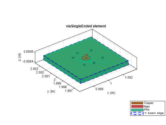
View the via.
show(via)

Create a single-ended via.
via = viaSingleEnded;
The signal layers for this board are on layers 1 and 5. The ground/return layers for this board are on layers 3, 7, and 9.
via.SignalLayer = [1 5];
via.GroundLayer = [3 7 9];
via.Substrate = dielectric("Name","FR4","EpsilonR",4.8,...
               "LossTangent",0.026,"Thickness",1.27e-4,"Frequency",1e8);
Create signal via location.
X = 1;
Y = 2;
start_layer = min(via.SignalLayer);
stop_layer = 7;
SVLocations = table(X, Y, start_layer, stop_layer)
SVLocations=1×4 table
    X    Y    start_layer    stop_layer
    _    _    ___________    __________

    1    2         1             7
via.SignalViaLocations = SVLocations.Variables;
Set two ports for the signal via 1 on layers 1 and 5 with trace width of 3e-4 m.
vPorts = table('Size',[2 4],'VariableTypes',["cell","cell","cell","cell"],...
    'VariableNames',["Signal Via Num", "Layer", "Trace Width", "Direction"]);
twidth = 3e-4;
vPorts(1,:) = {{1} {start_layer} {twidth} {45}};
vPorts(2,:) = {{1} {max(via.SignalLayer)} {twidth} {0}};
vPorts.Properties.RowNames = "Port #" + (1:size(vPorts,1))
vPorts=2×4 table
               Signal Via Num    Layer     Trace Width      Direction
               ______________    _____    ______________    _________

    Port #1        {[1]}         {[1]}    {[3.0000e-04]}     {[45]}
    Port #2        {[1]}         {[5]}    {[3.0000e-04]}     {[ 0]}
via.SignalTable = vPorts.Variables;
Create the ground return via locations.
via.GroundReturnViaLocations = [1.0015,2.001,start_layer, max(via.GroundLayer);...
    1.0015,1.999,start_layer, max(via.GroundLayer); ...
    0.999,1.999,start_layer, max(via.GroundLayer);...
    1,2.0015,start_layer, max(via.GroundLayer);...
    0.999,2.001,start_layer, max(via.GroundLayer);...
    1.0001,1.9987,start_layer, max(via.GroundLayer)]
via =
  viaSingleEnded with properties:

   Conducting Layers
                        SignalLayer: [1 5]
                        GroundLayer: [3 7 9]
                          Conductor: [1×1 metal]

   Dielectric Layers
                          Substrate: [1×1 dielectric]

   Signal Vias
                 SignalViaLocations: [1 2 1 7]
                  SignalViaDiameter: 2.5000e-04
          SignalViaFinishedDiameter: 2.0000e-04
                       SignalViaPad: [1×1 shape.Circle]
                   RemoveUnusedPads: 1
                   SignalViaAntipad: [1×1 shape.Circle]

   Ground Return Vias
           GroundReturnViaLocations: [6×4 double]
            GroundReturnViaDiameter: [6×1 double]
    GroundReturnViaFinishedDiameter: [6×1 double]

   Ports
                        SignalTable: {2×4 cell}
When SignalViaPad is a scalar, all pads use the same shape and size. View the pads information using padsTable:
padsTable(via)
ans=1×5 table
                          SignalPlane 1       GroundPlane 3      SignalPlane 5       GroundPlane 7    GroundPlane 9
                        __________________    _____________    __________________    _____________    _____________

    Signal Via Num 1    {1×1 shape.Circle}    {0×0 double}     {1×1 shape.Circle}    {0×0 double}     {0×0 double}
Note: To include pads on ground layers set 'RemoveUnusedPads' property to false.
To customize the pad on layer 5 (signal layer), get the cell-array of pad shapes using getpads:
pad_temp = getpads(via);
pad_temp{3}.Radius = 4.5e-4; % Customize the pad radius
via.SignalViaPad = pad_temp; % Assign it to the viaSingleEnded object
View the via.
show(via)
References
[1] Steinberger, Telian, Tsuk, Iyer and Yanamadala, “Proper Ground Via Placement for 40+ Gbps Signaling”, DesignCon 2022, April 2022.
[2] Ramo, Whinnery and Van Duzer, Fields and Waves in Communications Electronics, third edition, section 9.3, John Wiley and Sons Inc., copyright 1994